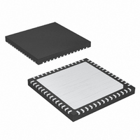
MAX8655ETN+T Maxim Integrated Products, MAX8655ETN+T Datasheet - Page 17

MAX8655ETN+T
Manufacturer Part Number
MAX8655ETN+T
Description
IC STEP-DN REG 25A 56-TQFN-EP
Manufacturer
Maxim Integrated Products
Type
Step-Down (Buck)r
Datasheet
1.MAX8655ETNT.pdf
(23 pages)
Specifications of MAX8655ETN+T
Internal Switch(s)
Yes
Synchronous Rectifier
No
Number Of Outputs
1
Voltage - Output
0.7 ~ 5.5 V
Current - Output
25A
Frequency - Switching
200kHz ~ 1MHz
Voltage - Input
4.5 ~ 25 V
Operating Temperature
-40°C ~ 85°C
Mounting Type
Surface Mount
Package / Case
56-TQFN Exposed Pad
Lead Free Status / RoHS Status
Lead free / RoHS Compliant
Power - Output
-
Lead Free Status / Rohs Status
Lead free / RoHS Compliant
Capacitor C11 is connected in parallel with R2 and is
equal in value with C9.
Add a 100pF (C10) capacitor across the CS+ and CS-
inputs close to the IC.
The input filter capacitor reduces peak currents drawn
from the power source and reduces noise and voltage
ripple on the input caused by the circuit’s switching.
The input capacitors must meet the ripple-current
requirement (I
defined by the following equation:
I
equals twice the output voltage (V
I
mended due to the low ESR and ESL at high frequency
with relatively low cost. Choose a capacitor that
exhibits less than 10°C temperature rise at the maxi-
mum operating RMS current for optimum long-term reli-
ability. Ceramic capacitors with an X5R or better
temperature characteristic are recommended.
The key selection parameters for the output capacitor
are the actual capacitance value, the equivalent series
resistance (ESR), the equivalent series inductance
(ESL), and the voltage-rating requirements. These
parameters affect the overall stability, output-voltage
ripple, and transient response. The output ripple has
three components: variations in the charge stored in
the output capacitor, the voltage drop across the
capacitor’s ESR, and ESL caused by the current into
and out of the capacitor. The maximum output-voltage
ripple is estimated as follows:
The output-voltage ripple as a consequence of the
ESR, ESL, and output capacitance is:
where I
RMS
RMS(MAX)
V
RIPPLE
has a maximum value when the input voltage
P-P
= V
I
RMS
is the peak-to-peak inductor current.
= I
V
RIPPLE(ESR)
RMS
LOAD
RIPPLE ESL
V
V
=
RIPPLE ESR
RIPPLE C
I
LOAD
______________________________________________________________________________________
) imposed by the switching currents
/2. Ceramic capacitors are recom-
Internal MOSFET, Step-Down Regulator
(
(
( )
V
)
+ V
=
OUT
)
=
8
=
L ESL
RIPPLE(C)
×
I
V
P P
+
V
IN
×
C
Highly Integrated, 25A, Wide-Input,
−
IN
I
(
P P
OUT
V
Output Capacitor
−
×
IN
ESR
Input Capacitor
IN
×
−
×
ESL
V
= 2 x V
f
+ V
S
OUT
RIPPLE(ESL)
)
OUT
), so
These equations are suitable for initial capacitor selec-
tion, but final values should be chosen based on a pro-
totype or evaluation circuit. As a general rule, a smaller
current ripple results in less output-voltage ripple.
Since the inductor ripple current is a factor of the
inductor value and input voltage, the output-voltage rip-
ple decreases with larger inductance, and increases
with higher input voltages. The MAX8655 is designed to
work with polymer, tantalum, aluminum electrolytic, or
ceramic output capacitors. The aluminum electrolytic
capacitor is the least expensive; however, it has higher
ESR. To compensate for this, use a ceramic capacitor
in parallel to reduce the switching ripple and noise.
Ceramic capacitors are recommended for high-fre-
quency (500kHz to 1MHz) designs. For reliable and
safe operation, ensure that the capacitor’s voltage and
ripple-current ratings exceed the calculated values.
The response to a load transient depends on the
selected output capacitors. During a load transient, the
output voltage instantly changes by ESR x ∆I
Before the regulator can respond, the output voltage
deviates further, depending on the inductor and output-
capacitor values. After a short time (see the Typical
Operating Characteristics section), the regulator
responds by regulating the output voltage back to its
nominal state. The regulator response time depends on
its closed-loop bandwidth. With a higher bandwidth,
the response time is faster, thus preventing the output
voltage from further deviation from its regulating value.
The MAX8655 uses an internal transconductance error
amplifier whose output compensates the control loop.
The external inductor, output capacitor, compensation
resistor, and compensation capacitors determine the
loop stability. The inductor and output capacitor are cho-
sen based on performance, size, and cost. Additionally,
the compensation resistor and capacitors are selected to
optimize control-loop stability. The component values,
shown in Figures 3 and 4, yield stable operation over the
given range of input-to-output voltages.
The regulator uses a current-mode control scheme that
regulates the output voltage by forcing the required cur-
rent through the external inductor. The voltage drop
across the DC resistance of the inductor or the alternate
series current-sense resistor is used to measure the
inductor current. Current-mode control eliminates the
double pole in the feedback loop caused by the
I
P P
−
=
V
IN
f
S
−
×
V
OUT
Compensation Design
L
×
V
OUT
V
IN
LOAD
17
.


