CDB5378 Cirrus Logic Inc, CDB5378 Datasheet - Page 19
CDB5378
Manufacturer Part Number
CDB5378
Description
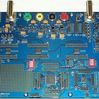
EVALUATION BOARD FOR CS5378
Manufacturer
Cirrus Logic Inc
Datasheets
1.CS5373A-ISZR.pdf
(40 pages)
2.CDB5378.pdf
(16 pages)
3.CDB5378.pdf
(74 pages)
4.CDB5378.pdf
(88 pages)
Specifications of CDB5378
Main Purpose
Seismic Evaluation System
Embedded
Yes, MCU, 8-Bit
Utilized Ic / Part
CS3301A, CS5373A, CS5378
Primary Attributes
Single Digital Filter
Secondary Attributes
Graphical User Interface, SPI™ & USB Interfaces
Processor To Be Evaluated
CS5378
Interface Type
USB
Lead Free Status / RoHS Status
Contains lead / RoHS non-compliant
Lead Free Status / RoHS Status
Lead free / RoHS Compliant, Contains lead / RoHS non-compliant


2. GENERAL DESCRIPTION
The CS5373A is a high-performance, fourth-
order ΔΣ modulator integrated with a digital-to-
analog converter (DAC). When combined with
a CS3301A/02A differential amplifier and the
CS5378 digital filter, a small low-power self-
testing high-accuracy single-channel mea-
surement system results.
2.1 Delta-Sigma Modulator
The CS5373A modulator has high dynamic
range and low total harmonic distortion with
very low power consumption, and is optimized
for extremely high-resolution measurement of
5 V
analog input signals between DC and 1720 Hz
to an oversampled serial bit stream at
512 kbits per second.
The CS5378 digital filter generates the clock
and synchronization inputs for the modulator
while receiving the modulator one-bit data and
over-range flag outputs. The digital filter then
decimates the modulator’s oversampled out-
put bit stream to a 24-bit output at the selected
output word rate.
2.2 Digital-to-Analog Converter
The CS5373A test DAC is driven by a digital
ΔΣ bit stream from the CS5378 digital filter’s
test bit stream (TBS) generator and operates
in either AC or DC test modes. AC test modes
DS703F2
pp
or smaller differential signals. It converts
OUT+
OUT-
BUF+
BUF-
INR+
INF+
INF-
INR-
Figure 6. CS5373A Block Diagram
VA+
VA-
VREF+
ATT(0, 1, 2)
Attenuator
Modulator
1/1 to 1/64
24-Bit
ΔΣ
VREF-
(MODE 1, 2, 3, 6) are used to measure sys-
tem THD and CMRR performance. DC test
modes (MODE 4, 5) are for gain calibration
and pulse tests. The digital filter also provides
clock and syncronization signals as well as
GPIO control signals to set the operational
mode and analog output attenuation.
Two sets of differential analog outputs, OUT
and BUF, simplify system design as dedicated
outputs for testing the electronics channel and
for in-circuit sensor tests. Output attenuator
settings are binary weighted (1, 1/2, 1/4, 1/8,
1/16, 1/32, 1/64) and match the CS3301A/02A
amplifier input levels for full-scale testing at all
gain ranges.
For maximum performance, the precision out-
puts (OUT±) must drive only high-impedance
loads such as the CS3301A/02A amplifier in-
puts. The buffered outputs (BUF±) can drive
lower-impedance loads, down to 1 kΩ, but with
reduced performance compared to the preci-
sion outputs.
The test DAC is optimized for low-power oper-
ation and has a restricted operational band-
width in the AC modes. For stable operation,
full-scale AC test signals must not contain fre-
quencies above 100 Hz. AC test signals above
100 Hz (TBS impulse mode, for example)
must have a -20 dB reduced amplitude to en-
sure stability of the low-power ΔΣ architecture.
MODE(0, 1, 2)
Generator
Test DAC
Clock
24-Bit
ΔΣ
GND
VD
MDATA
MFLAG
MCLK
MSYNC
TDATA
CAP+
CAP-
CS5373A
19
Related parts for CDB5378
Image
Part Number
Description
Manufacturer
Datasheet
Request
R

Part Number:
Description:
Development Kit
Manufacturer:
Cirrus Logic Inc
Datasheet:
Part Number:
Description:
Development Kit
Manufacturer:
Cirrus Logic Inc
Datasheet:


Part Number:
Description:
High-efficiency PFC + Fluorescent Lamp Driver Reference Design
Manufacturer:
Cirrus Logic Inc
Datasheet:
Part Number:
Description:
Development Kit
Manufacturer:
Cirrus Logic Inc
Datasheet:
Part Number:
Description:
Development Kit
Manufacturer:
Cirrus Logic Inc
Datasheet:

Part Number:
Description:
Development Kit
Manufacturer:
Cirrus Logic Inc
Datasheet:
Part Number:
Description:
Development Kit
Manufacturer:
Cirrus Logic Inc
Datasheet:
Part Number:
Description:
Development Kit
Manufacturer:
Cirrus Logic Inc
Datasheet:
Part Number:
Description:
Development Kit
Manufacturer:
Cirrus Logic Inc
Datasheet:

Part Number:
Description:
EVALUATION BOARD FOR CS8427
Manufacturer:
Cirrus Logic Inc
Datasheet:

Part Number:
Description:
BOARD EVAL FOR CS8416 RCVR
Manufacturer:
Cirrus Logic Inc
Datasheet:

Part Number:
Description:
EVALUATION BOARD FOR CS8420
Manufacturer:
Cirrus Logic Inc
Datasheet:

Part Number:
Description:
KIT DEVELOPMENT EP9315 ARM9
Manufacturer:
Cirrus Logic Inc
Datasheet:

Part Number:
Description:
KIT DEVELOPMENT EP9302 ARM9
Manufacturer:
Cirrus Logic Inc
Datasheet: