CDB5378 Cirrus Logic Inc, CDB5378 Datasheet - Page 28
CDB5378
Manufacturer Part Number
CDB5378
Description
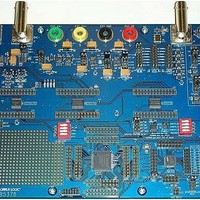
EVALUATION BOARD FOR CS5378
Manufacturer
Cirrus Logic Inc
Datasheets
1.CS5373A-ISZR.pdf
(40 pages)
2.CDB5378.pdf
(16 pages)
3.CDB5378.pdf
(74 pages)
4.CDB5378.pdf
(88 pages)
Specifications of CDB5378
Main Purpose
Seismic Evaluation System
Embedded
Yes, MCU, 8-Bit
Utilized Ic / Part
CS3301A, CS5373A, CS5378
Primary Attributes
Single Digital Filter
Secondary Attributes
Graphical User Interface, SPI™ & USB Interfaces
Processor To Be Evaluated
CS5378
Interface Type
USB
Lead Free Status / RoHS Status
Contains lead / RoHS non-compliant
Lead Free Status / RoHS Status
Lead free / RoHS Compliant, Contains lead / RoHS non-compliant


7. ANALOG SIGNALS
The CS5373A has multiple differential analog
inputs and outputs. The modulator analog in-
puts are separated into rough and fine charge
differential pairs (INR±, INF±) for maximum
sampling accuracy. Both sets of modulator in-
puts require a simple differential anti-alias RC
filter to ensure high-frequency signals do not
alias into the measurement bandwidth.
The test DAC has a precision differential out-
put (OUT±) that provides the best analog per-
formance, but with only minimal drive
capability. A buffered output (BUF±) can drive
an external load, but with reduced analog per-
formance. Finally, the test DAC internal anti-
alias filter requires a dedicated capacitor con-
nection (CAP±) to eliminate undesired high-
frequency signals.
7.1 INR±, INF± Modulator Inputs
The modulator analog inputs are separated
into differential rough and fine signals (INR±,
INF±). The positive half of the differential input
signal is connected to INR+ and INF+, while
the negative half is attached to INF- and INR-.
The INR± pins are switched-capacitor ‘rough
charge’ inputs that pre-charge the internal an-
alog sampling capacitor before it is connected
to the INF± fine input pins.
28
VA+
VA-
CS 3301 A/02 A
INPUT FROM
VREF
AM PLIFIER
2.5 V
ELECTRONICS
TEST OUTPUT
TEST OUTPUT
10 Ω
SENSOR
100 µF
680 Ω
680 Ω
680 Ω
680 Ω
Figure 14. Analog Signals
+
*Populate with 2 x 10 nF or
20 nF
1 x 22 nF C0 G or better .
C0G
Route VREF as diff pair
Route OUT as diff pair
Route BUF as diff pair
*
VA+
VA-
10 nF
C0 G
20 nF
C0 G
0. 1µF
0.1 µF
*
CAP +
CAP -
BUF+
BUF-
OUT+
OUT-
VREF +
VREF -
INR+
INF+
INF-
INR-
7.1.1
The modulator input has a dynamic switched-
capacitor architecture and so has a rough
charge input impedance that is inversely pro-
portional to the input master clock frequency
and the input capacitor size, [1 / (f * C)].
Internal to the modulator, the rough inputs
(INR±) pre-charge the sampling capacitor
used by the fine inputs (INF±), therefore the in-
put current to the fine inputs is very low and the
effective input impedance is orders of magni-
tude above the impedance of the rough inputs.
7.1.2
The modulator inputs are required to be band-
width limited to ensure modulator loop stability
and prevent high-frequency signals from alias-
ing into the measurement band. The use of
simple single-pole differential low-pass RC fil-
ters across the INR± and INF± inputs ensures
high-frequency signals are rejected before
they can alias into the measurement band.
•
•
•
VA +
VA -
CS5373A
MCLK = 2.048 MHz
INR± Input Cap = 20 pF
Impedance = [1 / (2.048 MHz * 20 pF)] = 24 kΩ.
M SYNC
GND
M DATA
M ODE0
M ODE1
M ODE2
M FLAG
Modulator Input Impedance
Modulator Anti-alias Filter
VD
TDATA
M CLK
ATT 0
ATT 1
ATT 2
0.1µF
GPIO
GPIO
GPIO
GPIO
GPIO
GPIO
TBSDATA
M CLK
M SYNC
M DATA
M FLAG
VD
SIGNALS
CS5378
CS5373A
DS703F2
Related parts for CDB5378
Image
Part Number
Description
Manufacturer
Datasheet
Request
R

Part Number:
Description:
Development Kit
Manufacturer:
Cirrus Logic Inc
Datasheet:
Part Number:
Description:
Development Kit
Manufacturer:
Cirrus Logic Inc
Datasheet:


Part Number:
Description:
High-efficiency PFC + Fluorescent Lamp Driver Reference Design
Manufacturer:
Cirrus Logic Inc
Datasheet:
Part Number:
Description:
Development Kit
Manufacturer:
Cirrus Logic Inc
Datasheet:
Part Number:
Description:
Development Kit
Manufacturer:
Cirrus Logic Inc
Datasheet:

Part Number:
Description:
Development Kit
Manufacturer:
Cirrus Logic Inc
Datasheet:
Part Number:
Description:
Development Kit
Manufacturer:
Cirrus Logic Inc
Datasheet:
Part Number:
Description:
Development Kit
Manufacturer:
Cirrus Logic Inc
Datasheet:
Part Number:
Description:
Development Kit
Manufacturer:
Cirrus Logic Inc
Datasheet:

Part Number:
Description:
EVALUATION BOARD FOR CS8427
Manufacturer:
Cirrus Logic Inc
Datasheet:

Part Number:
Description:
BOARD EVAL FOR CS8416 RCVR
Manufacturer:
Cirrus Logic Inc
Datasheet:

Part Number:
Description:
EVALUATION BOARD FOR CS8420
Manufacturer:
Cirrus Logic Inc
Datasheet:

Part Number:
Description:
KIT DEVELOPMENT EP9315 ARM9
Manufacturer:
Cirrus Logic Inc
Datasheet:

Part Number:
Description:
KIT DEVELOPMENT EP9302 ARM9
Manufacturer:
Cirrus Logic Inc
Datasheet: