KDC5514EVALZ Intersil, KDC5514EVALZ Datasheet - Page 17
KDC5514EVALZ
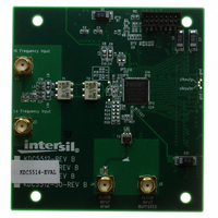
Manufacturer Part Number
KDC5514EVALZ
Description
DAUGHTER CARD FOR KAD5514
Manufacturer
Intersil
Series
FemtoCharge™r
Datasheets
1.KAD5514P-25Q72.pdf
(34 pages)
2.KMB-001LEVALZ.pdf
(7 pages)
3.KDC5514EVALZ.pdf
(9 pages)
Specifications of KDC5514EVALZ
Number Of Adc's
1
Number Of Bits
14
Sampling Rate (per Second)
250M
Data Interface
Parallel
Inputs Per Adc
1 Differential
Input Range
1.47 Vpp
Power (typ) @ Conditions
429mW @ 250MSPS
Voltage Supply Source
Single Supply
Operating Temperature
-40°C ~ 85°C
Utilized Ic / Part
KAD5514P-25, KMB001 Motherboard
For Use With
KMB001LEVAL - MOTHERBOARD FOR LVDS ADC CARD
Lead Free Status / RoHS Status
Lead free / RoHS Compliant
Other names
KDC5514EVAL
KDC5514EVAL
KDC5514EVAL
Available stocks
Company
Part Number
Manufacturer
Quantity
Price
Company:

Part Number:
KDC5514EVALZ
Manufacturer:
Intersil
Quantity:
5


Theory of Operation
Functional Description
The KAD5514P is based upon a 12-bit, 250MSPS A/D
converter core that utilizes a pipelined successive
approximation architecture (Figure 23). The input voltage is
captured by a Sample-Hold Amplifier (SHA) and converted
to a unit of charge. Proprietary charge-domain techniques
are used to successively compare the input to a series of
reference charges. Decisions made during the successive
approximation operations determine the digital code for each
input value. The converter pipeline requires six samples to
produce a result. Digital error correction is also applied,
resulting in a total latency of seven and one half clock cycles.
This is evident to the user as a time lag between the start of
a conversion and the data being available on the digital
outputs.
The KAD5514P family operates by simultaneously sampling
the input signal with two ADC cores in parallel and summing
the digital result. Since the input signal is correlated between
the two cores and noise is not, an increase in SNR is
achieved. As a result of this architecture, indexed SPI
operations must be executed on each core in series. Refer
to “Indexed Device Configuration/Control” on page 24 for
more details.
INN
INP
1.25V
17
SHA
+
–
FIGURE 23. ADC CORE BLOCK DIAGRAM
2.5-BIT
FLASH
KAD5514P
1.5-BIT/STAGE
6-STAGE
Power-On Calibration
The ADC performs a self-calibration at start-up. An internal
power-on-reset (POR) circuit detects the supply voltage
ramps and initiates the calibration when the analog and
digital supply voltages are above a threshold. The following
conditions must be adhered to for the power-on calibration to
execute successfully:
• A frequency-stable conversion clock must be applied to
• DNC pins (especially 3, 4 and 18) must not be pulled up or
• SDO (pin 66) must be high
• RESETN (pin 25) must begin low
• SPI communications must not be attempted
A user-initiated reset can subsequently be invoked in the
event that the above conditions cannot be met at power-up.
The SDO pin requires an external 4.7kΩ pull-up to OVDD. If
the SDO pin is pulled low externally during power-up,
calibration will not be executed properly.
After the power supply has stabilized the internal POR
releases RESETN and an internal pull-up pulls it high, which
starts the calibration sequence. If a subsequent
user-initiated reset is required, the RESETN pin should be
connected to an open-drain driver with a drive strength of
less than 0.5mA.
LVDS/LVCMOS
GENERATION
CORRECTION
the CLKP/CLKN pins
down
OUTPUTS
DIGITAL
CLOCK
ERROR
1-BIT/STAGE
3-STAGE
FLASH
3-BIT
September 10, 2009
FN6804.2
Related parts for KDC5514EVALZ
Image
Part Number
Description
Manufacturer
Datasheet
Request
R

Part Number:
Description:
DAUGHTER CARD FOR KAD5514
Manufacturer:
Intersil
Datasheet:

Part Number:
Description:
Intersil Corporation [CMOS Serial Controller Interface]
Manufacturer:
Intersil Corporation
Datasheet:
Part Number:
Description:
Manufacturer:
Intersil Corporation
Datasheet:
Part Number:
Description:
357-036-542-201 CARDEDGE 36POS DL .156 BLK LOPRO
Manufacturer:
Intersil Corporation
Datasheet:
Part Number:
Description:
1024-Word x 4-Bit LSI Static RAM
Manufacturer:
Intersil Corporation
Datasheet:
Part Number:
Description:
General Purpose NPN Transistor Arrays FN341.4
Manufacturer:
Intersil Corporation
Datasheet:
Part Number:
Description:
CMOS 16-Bit Microprocessor
Manufacturer:
Intersil Corporation
Datasheet:
Part Number:
Description:
Manufacturer:
Intersil Corporation
Datasheet:
Part Number:
Description:
Manufacturer:
Intersil Corporation
Datasheet:
Part Number:
Description:
Manufacturer:
Intersil Corporation
Datasheet:
Part Number:
Description:
Manufacturer:
Intersil Corporation
Datasheet:
Part Number:
Description:
CMOS 6-Bit Latch and Decoder Memory Interfaces
Manufacturer:
Intersil Corporation
Datasheet:
Part Number:
Description:
CA3046General Purpose NPN Transistor Arrays
Manufacturer:
Intersil Corporation
Datasheet:
Part Number:
Description:
Manufacturer:
Intersil Corporation
Datasheet:
Part Number:
Description:
TR909 DLC/FLC SLIC with Low Power Standby
Manufacturer:
Intersil Corporation
Datasheet: