EVAL-AD7689EDZ Analog Devices Inc, EVAL-AD7689EDZ Datasheet - Page 2
EVAL-AD7689EDZ
Manufacturer Part Number
EVAL-AD7689EDZ
Description
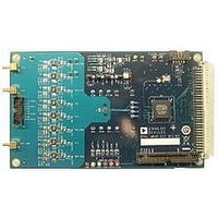
BOARD EVAL AD7689
Manufacturer
Analog Devices Inc
Series
PulSAR®r
Specifications of EVAL-AD7689EDZ
Number Of Adc's
1
Number Of Bits
16
Sampling Rate (per Second)
250k
Data Interface
Serial
Inputs Per Adc
8 Single Ended
Input Range
±VREF
Power (typ) @ Conditions
12.5mW @ 250kSPS, 5 V
Voltage Supply Source
Single Supply
Operating Temperature
-40°C ~ 85°C
Utilized Ic / Part
AD7689
Silicon Manufacturer
Analog Devices
Application Sub Type
ADC
Kit Application Type
Data Converter
Silicon Core Number
AD7689
Lead Free Status / RoHS Status
Lead free / RoHS Compliant


EVAL-AD76MUXEDZ
TABLE OF CONTENTS
Features .............................................................................................. 1
Revision History ............................................................................... 2
LIST OF FIGURES
Figure 1.Evaluation Board ............................................................... 1
Figure 2. Setup Screen ...................................................................... 8
Figure 3. Default CFG ..................................................................... 9
Figure 4. CGF Enable/Disable Selection....................................... 9
Figure 5. Input Configuration/Channel Selection........................ 9
Figure 6.BW Select............................................................................ 9
Figure 7. Reference Selection .......................................................... 9
Figure 8. Context Help, User Controls ......................................... 10
Figure 9. Histogram Screen ........................................................... 11
Figure 10. Summary ....................................................................... 12
Figure 11. FFT Spectrum ............................................................... 13
Figure 12 .Oscilloscope .................................................................. 14
Figure 13. Schematic, ADC + Block Diagram............................. 15
LIST OF TABLES
Table 1. Jumper Description............................................................ 6
Table 2.Test Points ............................................................................ 7
REVISION HISTORY
Overview........................................................................................ 3
Conversion Control...................................................................... 3
Analog Inputs................................................................................ 3
Serial Interface .............................................................................. 3
Reference ....................................................................................... 3
Power Supplies and Grounding .................................................. 3
Schematics/PCB Layout............................................................... 4
Hardware Setup ............................................................................ 4
Rev. PrD | Page 2 of 26
Figure 14. Schematic, Supplies ...................................................... 16
Figure 15. Schematic, Reference, Buffer, V
Figure 16. Schematic, AnalogCH0-CH3...................................... 18
Figure 17. Schematic, AnalogCH4-CH7...................................... 19
Figure 18. Schematic, FPGA.......................................................... 20
Figure 19. Schematic, 96-Pin Interface ........................................ 21
Figure 20. Top Side Silk-Screen .................................................... 22
Figure 21. Inner Layer 1................................................................. 22
Figure 22. Ground Plane................................................................ 23
Figure 23. Inner Layer 2................................................................. 23
Figure 24.Inner Layer 3.................................................................. 24
Figure 25. Bottom Layer ................................................................ 24
Figure 26. Bottom Layer ................................................................ 25
Table 3. Bill of Materials for the Connectors .................................7
Software Installation .....................................................................4
Running the Evaluation Software ..............................................5
Setup Screen...................................................................................5
Configuring the ADC ...................................................................5
DC Testing - Histogram ...............................................................5
AC Testing ......................................................................................5
Software Operation .......................................................................8
ADC Configuration ......................................................................9
Evaluation Board Schematics and Artwork............................ 15
Ordering Guide .......................................................................... 26
Preliminary Technical Data
CM
, V
BIAS
.................... 17
Related parts for EVAL-AD7689EDZ
Image
Part Number
Description
Manufacturer
Datasheet
Request
R


Part Number:
Description:
BOARD EVAL FOR SI270X-A
Manufacturer:
Silicon Laboratories Inc
Datasheet:

Part Number:
Description:
BUCK CONV REF DESIGN KIT IP1201
Manufacturer:
International Rectifier
Datasheet:
Part Number:
Description:
BOARD DEMO SYNC DUAL BUCK CNVTER
Manufacturer:
International Rectifier
Datasheet:
Part Number:
Description:
BOARD DEMO SYNC BUCK CONVETER
Manufacturer:
International Rectifier
Datasheet:

Part Number:
Description:
EVALBOARD/EB Omnidirectional microphone - Analog
Manufacturer:
Analog Devices
Datasheet:
Part Number:
Description:
EVALBOARD/EB Omnidirectional microphone - Analog
Manufacturer:
Analog Devices
Datasheet:


Part Number:
Description:
BOARD EVAL LED DRIVER LT3756
Manufacturer:
Linear Technology
Datasheet:

Part Number:
Description:
BOARD EVAL FOR AD7741/7742
Manufacturer:
Analog Devices Inc
Datasheet:

Part Number:
Description:
±1.7g Dual-Axis IMEMS Accelerometer Evaluation Board
Manufacturer:
Analog Devices Inc
Datasheet:

Part Number:
Description:
IC MULTIPLIER ANALOG 8-SOIC T/R
Manufacturer:
Analog Devices Inc
Datasheet:

Part Number:
Description:
IC ANALOG MULTIPLIER 8-DIP
Manufacturer:
Analog Devices Inc
Datasheet:
Part Number:
Description:
IC ANALOG MULTIPLIER 8-SOIC
Manufacturer:
Analog Devices Inc
Datasheet:
Part Number:
Description:
IC ANALOG MULTIPLIER 8-DIP
Manufacturer:
Analog Devices Inc
Datasheet: