EVAL-AD7689EDZ Analog Devices Inc, EVAL-AD7689EDZ Datasheet - Page 3
EVAL-AD7689EDZ
Manufacturer Part Number
EVAL-AD7689EDZ
Description
BOARD EVAL AD7689
Manufacturer
Analog Devices Inc
Series
PulSAR®r
Specifications of EVAL-AD7689EDZ
Number Of Adc's
1
Number Of Bits
16
Sampling Rate (per Second)
250k
Data Interface
Serial
Inputs Per Adc
8 Single Ended
Input Range
±VREF
Power (typ) @ Conditions
12.5mW @ 250kSPS, 5 V
Voltage Supply Source
Single Supply
Operating Temperature
-40°C ~ 85°C
Utilized Ic / Part
AD7689
Silicon Manufacturer
Analog Devices
Application Sub Type
ADC
Kit Application Type
Data Converter
Silicon Core Number
AD7689
Lead Free Status / RoHS Status
Lead free / RoHS Compliant


Preliminary Technical Data
OVERVIEW
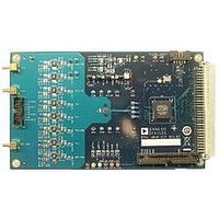
Figure 1 shows the EVAL-AD76MUXCBZ evaluation board.
When used in conjunction with the EVAL-CED1Z, the FPGA,
U6, provides the necessary control signals for conversion and
buffers the ADC serial output data into 16-bit wide transfers.
The evaluation board is a flexible design that enables the user to
choose among many different board configurations, analog
signal conditioning, reference, and different interfaces for
conversion results.
In stand alone operation, the FPGA can be used to buffer the 4-
wire interface via. P3, or directly to the 4 digital interface test
points SDO, SCK, DIN and CNV. For stand alone mode, supply
power to the evaluation board as detailed in the Power Supplies
and Grounding section below.
For FPGA buffered serial interface, supplying power is all that is
necessary. For direct serial connection to the ADC, place a
jumper across P3-39 and P3-40 as P3-40 pulled low places the
FPGA into high impedance.
CONVERSION CONTROL
Conversion start (CNV) controls the sample rate of the ADC
and is the only input needed for conversion; all SAR timing is
internally generated on the ADC. CNV is generated by the gate
array and the frequency is selected with the software.
While the ADC is converting, activity is indicated by the green
LED, CR1. Operating the software in Burst mode as opposed to
Continuous mode, will only light the LED when conversion is
taking place.
For stand alone operation, connect a low jitter source to either
P3-8 or CNV.
ANALOG INPUTS
SMB connectors, J1 and J2, are provided for the ADC input
channels IN0 and IN1 (IN0 only on AD7682). These inputs are
also on the IDC connector P1-2 and P1-4. The remaining inputs
are also on P1-6 through P1-16 (even pins only). J3 can be
configured for providing a common point (COM) for all input
signals or for any analog input IN0-IN7. For using J3 as an
external common point, remove the solder pad (bottom of
PCB) from “COMS to COM” and solder “EXT_COM to COM”
as shown below.
To configure J3 to drive any of the analog input channels,
remove R35 from the left pads (bottom of PCB) and solder it to
the rightmost pads.
Rev. PrD | Page 3 of 26
The analog input amplifier circuitry U13 – U20 (see schematic -
Figure 13) allows flexible configuration changes such as positive
or negative gain, input range scaling, filtering, addition of a DC
component, use of different op-amp and supplies. The analog
input amplifiers are set as unity gain buffers at the factory. The
supplies are selectable with solder pads VDRV- and VDRV+
and are set for the +7V, -5V range.
Note that when using the unipolar configuration, COMS (P8) is
set to (P8, 2-3) and for bipolar input configuration set to (P8, 1-
2) with pin 1 being the leftmost pin.
SERIAL INTERFACE
The 3-wire serial interface DIN, SCK, and SDO along with CNV
are present on the digital interface test points and FPGA
buffered versions are on the 40-pin IDC connector, P3-2, -4, -6,
-8. When connected to the EVAL-CED1Z and stand alone
(without P3-39 to P3-40 jumper), signals are present at both
locations. With P3-39 to P3-40 connected, these signals are only
present at the test points SDO, SCK DIN and CNV.
REFERENCE
All of the ADCs for this evaluation board can use a precision
trimmed on-chip band gap reference, an on-board precision
ADR435 band gap reference, or an external reference connected
to the EXTREF test point (TP17). The on-chip reference is
enabled or disabled with the software. The on-chip reference
can be set for 2.5V or 4.096V outputs and also includes an
internal buffer, useful for external reference applications. When
using the on-chip reference, remove the jumper on TP7 since
this will overdrive the on-chip reference with the external one.
The default configuration is for on-board ADR435 reference
with a buffered output (P5 2-3), (P6 1-2) and (P7 1-2).
For using an external reference connect to the EXTREF test
point (TP17), select a buffer or not with P6 and select if driving
the ADC REF directly or using the ADC’s internal reference
buffer. When using the internal reference buffer with gain=1,
the maximum output is limited to 4.096V (headroom from 5V
supply).
The default configuration sets the amplifiers output to be at
V
POWER SUPPLIES AND GROUNDING
To attain high resolution performance, the board was designed
to ensure that all digital ground return paths do not cross the
analog ground return paths by connecting the planes together
directly under the converter. Power is supplied to the board
through P3 when using with the EVAL-CED1Z. For stand alone
REF
/2 (mid-scale) from the voltage divider at U1B (V
EVAL-AD76MUXEDZ
BIAS
).
Related parts for EVAL-AD7689EDZ
Image
Part Number
Description
Manufacturer
Datasheet
Request
R


Part Number:
Description:
BOARD EVAL FOR SI270X-A
Manufacturer:
Silicon Laboratories Inc
Datasheet:

Part Number:
Description:
BUCK CONV REF DESIGN KIT IP1201
Manufacturer:
International Rectifier
Datasheet:
Part Number:
Description:
BOARD DEMO SYNC DUAL BUCK CNVTER
Manufacturer:
International Rectifier
Datasheet:
Part Number:
Description:
BOARD DEMO SYNC BUCK CONVETER
Manufacturer:
International Rectifier
Datasheet:

Part Number:
Description:
EVALBOARD/EB Omnidirectional microphone - Analog
Manufacturer:
Analog Devices
Datasheet:
Part Number:
Description:
EVALBOARD/EB Omnidirectional microphone - Analog
Manufacturer:
Analog Devices
Datasheet:


Part Number:
Description:
BOARD EVAL LED DRIVER LT3756
Manufacturer:
Linear Technology
Datasheet:

Part Number:
Description:
BOARD EVAL FOR AD7741/7742
Manufacturer:
Analog Devices Inc
Datasheet:

Part Number:
Description:
±1.7g Dual-Axis IMEMS Accelerometer Evaluation Board
Manufacturer:
Analog Devices Inc
Datasheet:

Part Number:
Description:
IC MULTIPLIER ANALOG 8-SOIC T/R
Manufacturer:
Analog Devices Inc
Datasheet:

Part Number:
Description:
IC ANALOG MULTIPLIER 8-DIP
Manufacturer:
Analog Devices Inc
Datasheet:
Part Number:
Description:
IC ANALOG MULTIPLIER 8-SOIC
Manufacturer:
Analog Devices Inc
Datasheet:
Part Number:
Description:
IC ANALOG MULTIPLIER 8-DIP
Manufacturer:
Analog Devices Inc
Datasheet: