EVAL-AD7612CBZ Analog Devices Inc, EVAL-AD7612CBZ Datasheet - Page 10
EVAL-AD7612CBZ
Manufacturer Part Number
EVAL-AD7612CBZ
Description
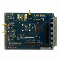
BOARD EVALUATION FOR AD7612
Manufacturer
Analog Devices Inc
Series
PulSAR®r
Specifications of EVAL-AD7612CBZ
Number Of Adc's
1
Number Of Bits
16
Sampling Rate (per Second)
750k
Data Interface
Serial, Parallel
Inputs Per Adc
1 Single Ended
Input Range
±5 V, ±10 V
Power (typ) @ Conditions
205mW @ 750kSPS
Voltage Supply Source
Analog and Digital
Operating Temperature
-40°C ~ 85°C
Utilized Ic / Part
AD7612
Lead Free Status / RoHS Status
Lead free / RoHS Compliant


AD7612
Pin No.
24
25
26
27
28
29
30
31
32
33
34
35
36
37
38
39
40
41
Mnemonic
D11 or
RDERROR
D12 or
HW/SW
D13 or
SCIN
D14 or
SCCLK
D15 or
SCCS
BUSY
TEN
RD
CS
RESET
PD
CNVST
BIPOLAR
REF
REFGND
IN−
VCC
VEE
Type
DO
DI/O
DI/O
DI/O
DI/O
DO
DI
DI
DI
DI
DI
DI
DI
AI/O
AI
AI
P
P
2
2
2
1
Description
In parallel mode, this output is used as Bit 11 of the parallel port data output bus.
Serial Data Read Error. In serial slave mode (SER/PAR = high, EXT/INT = high), this output is used as an
incomplete data read error flag. If a data read is started and not completed when the current
conversion is complete, the current data is lost and RDERROR is pulsed high.
In parallel mode, this output is used as Bit 12 of the parallel port data output bus.
Serial Configuration Hardware/Software Select. In serial mode, this input is used to configure
the AD7612 by hardware or software. See the Hardware Configuration section and Software
Configuration section.
When HW/SW = low, the AD7612 is configured through software using the serial configuration register.
When HW/SW = high, the AD7612 is configured through dedicated hardware input pins.
In parallel mode, this output is used as Bit 13 of the parallel port data output bus.
Serial Configuration Data Input. In serial software configuration mode (SER/PAR = high, HW/SW = low)
this input is used to serially write in, MSB first, the configuration data into the serial configuration
register. The data on this input is latched with SCCLK. See the Software Configuration section.
In parallel mode, this output is used as Bit 14 of the parallel port data output bus.
Serial Configuration Clock. In serial software configuration mode (SER/PAR = high, HW/SW = low) this
input is used to clock in the data on SCIN. The active edge where the data SCIN is updated depends on
the logic state of the INVSCLK pin. See the Software Configuration section.
In parallel mode, this output is used as Bit 15 of the parallel port data output bus.
Serial Configuration Chip Select. In serial software configuration mode (SER/PAR = high, HW/SW = low)
this input enables the serial configuration port. See the Software Configuration section.
Busy Output. Transitions high when a conversion is started, and remains high until the conversion
is complete and the data is latched into the on-chip shift register. The falling edge of BUSY can be
used as a data ready clock signal. Note that in master read after convert mode (SER/PAR = high,
EXT/INT = low, RDC = low) the busy time changes according to Table 4.
Input Range Select. Used in conjunction with BIPOLAR per the following:
Read Data. When CS and RD are both low, the interface parallel or serial output bus is enabled.
Chip Select. When CS and RD are both low, the interface parallel or serial output bus is enabled. CS is
also used to gate the external clock in slave serial mode (not used for serial programmable port).
Reset Input. When high, reset the AD7612. Current conversion, if any, is aborted. The falling edge of
RESET resets the data outputs to all zero’s (with OB/2C = high) and clears the configuration register.
See the Digital Interface section. If not used, this pin can be tied to OGND.
Power-Down Input. When PD = high, power down the ADC. Power consumption is reduced and
conversions are inhibited after the current one is completed. The digital interface remains active
during power down.
Conversion Start. A falling edge on CNVST puts the internal sample-and-hold into the hold state and
initiates a conversion.
Input Range Select. See description for Pin 30.
Reference Input/Output.
When PDREF/PDBUF = low, the internal reference and buffer are enabled, producing 5 V on this pin.
When PDREF/PDBUF = high, the internal reference and buffer are disabled, allowing an externally
supplied voltage reference up to AVDD volts. Decoupling with at least a 22 μF is required with or
without the internal reference and buffer. See the Reference Decoupling section.
Reference Input Analog Ground. Connected to analog ground plane.
Analog Input Ground Sense. Should be connected to the analog ground plane or to a remote sense ground.
High Voltage Positive Supply. Normally +7 V to +15 V.
High Voltage Negative Supply. Normally 0 V to −15 V (0 V in unipolar ranges).
Input Range
0 V to 5 V
0 V to 10 V
±5 V
±10 V
BIPOLAR
Low
Low
High
High
Rev. 0 | Page 10 of 32
TEN
Low
High
Low
High
Related parts for EVAL-AD7612CBZ
Image
Part Number
Description
Manufacturer
Datasheet
Request
R


Part Number:
Description:
BOARD EVAL FOR SI270X-A
Manufacturer:
Silicon Laboratories Inc
Datasheet:

Part Number:
Description:
BUCK CONV REF DESIGN KIT IP1201
Manufacturer:
International Rectifier
Datasheet:
Part Number:
Description:
BOARD DEMO SYNC DUAL BUCK CNVTER
Manufacturer:
International Rectifier
Datasheet:
Part Number:
Description:
BOARD DEMO SYNC BUCK CONVETER
Manufacturer:
International Rectifier
Datasheet:

Part Number:
Description:
EVALBOARD/EB Omnidirectional microphone - Analog
Manufacturer:
Analog Devices
Datasheet:
Part Number:
Description:
EVALBOARD/EB Omnidirectional microphone - Analog
Manufacturer:
Analog Devices
Datasheet:


Part Number:
Description:
BOARD EVAL LED DRIVER LT3756
Manufacturer:
Linear Technology
Datasheet:

Part Number:
Description:
BOARD EVAL FOR AD7741/7742
Manufacturer:
Analog Devices Inc
Datasheet:

Part Number:
Description:
±1.7g Dual-Axis IMEMS Accelerometer Evaluation Board
Manufacturer:
Analog Devices Inc
Datasheet:

Part Number:
Description:
IC MULTIPLIER ANALOG 8-SOIC T/R
Manufacturer:
Analog Devices Inc
Datasheet:

Part Number:
Description:
IC ANALOG MULTIPLIER 8-DIP
Manufacturer:
Analog Devices Inc
Datasheet:
Part Number:
Description:
IC ANALOG MULTIPLIER 8-SOIC
Manufacturer:
Analog Devices Inc
Datasheet:
Part Number:
Description:
IC ANALOG MULTIPLIER 8-DIP
Manufacturer:
Analog Devices Inc
Datasheet: