EVAL-AD7612CBZ Analog Devices Inc, EVAL-AD7612CBZ Datasheet - Page 6
EVAL-AD7612CBZ
Manufacturer Part Number
EVAL-AD7612CBZ
Description
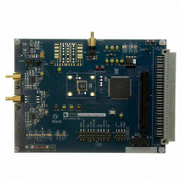
BOARD EVALUATION FOR AD7612
Manufacturer
Analog Devices Inc
Series
PulSAR®r
Specifications of EVAL-AD7612CBZ
Number Of Adc's
1
Number Of Bits
16
Sampling Rate (per Second)
750k
Data Interface
Serial, Parallel
Inputs Per Adc
1 Single Ended
Input Range
±5 V, ±10 V
Power (typ) @ Conditions
205mW @ 750kSPS
Voltage Supply Source
Analog and Digital
Operating Temperature
-40°C ~ 85°C
Utilized Ic / Part
AD7612
Lead Free Status / RoHS Status
Lead free / RoHS Compliant


AD7612
Parameter
SLAVE SERIAL/SERIAL CONFIGURATION INTERFACE MODES
Figure 43, and Figure 45)
1
2
3
Table 4. Serial Clock Timings in Master Read After Convert Mode
DIVSCLK[1]
DIVSCLK[0]
SYNC to SDCLK First Edge Delay Minimum
Internal SDCLK Period Minimum
Internal SDCLK Period Maximum
Internal SDCLK High Minimum
Internal SDCLK Low Minimum
SDOUT Valid Setup Time Minimum
SDOUT Valid Hold Time Minimum
SDCLK Last Edge to SYNC Delay Minimum
BUSY High Width Maximum
In warp mode only, the time between conversions is 1 ms; otherwise, there is no required maximum time.
In serial interface modes, the SDSYNC, SDSCLK, and SDOUT timings are defined with a maximum load C
In serial master read during convert mode. See Table 4 for serial master read after convert mode.
External SDCLK, SCCLK Setup Time
External SDCLK Active Edge to SDOUT Delay
SDIN/SCIN Setup Time
SDIN/SCIN Hold Time
External SDCLK/SCCLK Period
External SDCLK/SCCLK High
External SDCLK/SCCLK Low
Warp Mode
Normal Mode
Impulse Mode
TO OUTPUT
NOTES
1. IN SERIAL INTERFACE MODES, THE SYNC, SCLK, AND
SDOUT ARE DEFINED WITH A MAXIMUM LOAD
C
L
Figure 2. Load Circuit for Digital Interface Timing,
OF 10pF; OTHERWISE, THE LOAD IS 60pF MAXIMUM.
SDOUT, SYNC, and SCLK Outputs, C
PIN
60pF
C
L
1.6mA
500µA
I
I
OL
OH
1.4V
L
= 10 pF
2
(See Figure 42,
Rev. 0 | Page 6 of 32
Symbol
t
t
t
t
t
t
t
t
t
18
19
19
20
21
22
23
24
28
Symbol
t
t
t
t
t
t
t
31
32
33
34
35
36
37
0
0
3
30
45
15
10
4
5
5
1.65
1.9
2.15
t
DELAY
0.8V
Min
5
2
5
5
25
10
10
L
of 10 pF; otherwise, the load is 60 pF maximum.
Figure 3. Voltage Reference Levels for Timing
0
1
20
60
90
30
25
20
8
7
2.35
2.6
2.85
2V
0.8V
Typ
1
0
20
120
180
60
55
20
35
35
3.75
4.00
4.25
2V
Max
18
1
1
20
240
360
120
115
20
90
90
6.53
6.78
7.03
t
2V
0.8V
DELAY
Unit
ns
ns
ns
ns
ns
ns
ns
ns
μs
μs
μs
Unit
ns
ns
ns
ns
ns
ns
ns
Related parts for EVAL-AD7612CBZ
Image
Part Number
Description
Manufacturer
Datasheet
Request
R


Part Number:
Description:
BOARD EVAL FOR SI270X-A
Manufacturer:
Silicon Laboratories Inc
Datasheet:

Part Number:
Description:
BUCK CONV REF DESIGN KIT IP1201
Manufacturer:
International Rectifier
Datasheet:
Part Number:
Description:
BOARD DEMO SYNC DUAL BUCK CNVTER
Manufacturer:
International Rectifier
Datasheet:
Part Number:
Description:
BOARD DEMO SYNC BUCK CONVETER
Manufacturer:
International Rectifier
Datasheet:

Part Number:
Description:
EVALBOARD/EB Omnidirectional microphone - Analog
Manufacturer:
Analog Devices
Datasheet:
Part Number:
Description:
EVALBOARD/EB Omnidirectional microphone - Analog
Manufacturer:
Analog Devices
Datasheet:


Part Number:
Description:
BOARD EVAL LED DRIVER LT3756
Manufacturer:
Linear Technology
Datasheet:

Part Number:
Description:
BOARD EVAL FOR AD7741/7742
Manufacturer:
Analog Devices Inc
Datasheet:

Part Number:
Description:
±1.7g Dual-Axis IMEMS Accelerometer Evaluation Board
Manufacturer:
Analog Devices Inc
Datasheet:

Part Number:
Description:
IC MULTIPLIER ANALOG 8-SOIC T/R
Manufacturer:
Analog Devices Inc
Datasheet:

Part Number:
Description:
IC ANALOG MULTIPLIER 8-DIP
Manufacturer:
Analog Devices Inc
Datasheet:
Part Number:
Description:
IC ANALOG MULTIPLIER 8-SOIC
Manufacturer:
Analog Devices Inc
Datasheet:
Part Number:
Description:
IC ANALOG MULTIPLIER 8-DIP
Manufacturer:
Analog Devices Inc
Datasheet: