EVAL-AD7612CBZ Analog Devices Inc, EVAL-AD7612CBZ Datasheet - Page 23
EVAL-AD7612CBZ
Manufacturer Part Number
EVAL-AD7612CBZ
Description
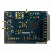
BOARD EVALUATION FOR AD7612
Manufacturer
Analog Devices Inc
Series
PulSAR®r
Specifications of EVAL-AD7612CBZ
Number Of Adc's
1
Number Of Bits
16
Sampling Rate (per Second)
750k
Data Interface
Serial, Parallel
Inputs Per Adc
1 Single Ended
Input Range
±5 V, ±10 V
Power (typ) @ Conditions
205mW @ 750kSPS
Voltage Supply Source
Analog and Digital
Operating Temperature
-40°C ~ 85°C
Utilized Ic / Part
AD7612
Lead Free Status / RoHS Status
Lead free / RoHS Compliant


Power Sequencing
The AD7612 is independent of power supply sequencing and is
very insensitive to power supply variations on AVDD over a wide
frequency range as shown in Figure 31.
Power Dissipation vs. Throughput
In impulse mode, the AD7612 automatically reduces its power
consumption at the end of each conversion phase. During the
acquisition phase, the operating currents are very low, which allows
a significant power savings when the conversion rate is reduced
(see Figure 32). This feature makes the AD7612 ideal for very
low power, battery-operated applications.
It should be noted that the digital interface remains active even
during the acquisition phase. To reduce the operating digital supply
currents even further, drive the digital inputs close to the power
rails (that is, OVDD and OGND).
1000
100
80
75
70
65
60
55
50
45
40
35
30
10
1
1
1
PDREF = PDBUF = HIGH
WARP MODE POWER
IMPULSE MODE POWER
Figure 32. Power Dissipation vs. Sample Rate
Figure 31. AVDD PSRR vs. Frequency
10
EXT REF
INT REF
SAMPLING RATE (kSPS)
10
FREQUENCY (kHz)
100
100
1000
10000
1000
Rev. 0 | Page 23 of 32
Power Down
Setting PD = high powers down the AD7612, thus reducing
supply currents to their minimums as shown in Figure 23. When
the ADC is in power down, the current conversion (if any) is
completed and the digital bus remains active. To further reduce
the digital supply currents, drive the inputs to OVDD or OGND.
Power down can also be programmed with the configuration
register. See the Software Configuration section for details. Note
that when using the configuration register, the PD input is a
don’t care and should be tied to either high or low.
CONVERSION CONTROL
The AD7612 is controlled by the CNVST input. A falling edge
on CNVST is all that is necessary to initiate a conversion. Detailed
timing diagrams of the conversion process are shown in Figure 33.
Once initiated, it cannot be restarted or aborted, even by the
power-down input, PD, until the conversion is complete. The
CNVST signal operates independently of CS and RD signals.
Although CNVST is a digital signal, it should be designed with
special care with fast, clean edges, and levels with minimum
overshoot, undershoot, or ringing.
The CNVST trace should be shielded with ground and a low value
(such as 50 Ω) serial resistor termination should be added close
to the output of the component that drives this line.
For applications where SNR is critical, the CNVST signal should
have very low jitter. This can be achieved by using a dedicated
oscillator for CNVST generation, or by clocking CNVST with a
high frequency, low jitter clock, as shown in Figure 27.
CNVST
MODE
BUSY
ACQUIRE
t
t
3
5
t
Figure 33. Basic Conversion Timing
1
CONVERT
t
7
t
4
t
2
t
6
ACQUIRE
t
8
AD7612
CONVERT
Related parts for EVAL-AD7612CBZ
Image
Part Number
Description
Manufacturer
Datasheet
Request
R


Part Number:
Description:
BOARD EVAL FOR SI270X-A
Manufacturer:
Silicon Laboratories Inc
Datasheet:

Part Number:
Description:
BUCK CONV REF DESIGN KIT IP1201
Manufacturer:
International Rectifier
Datasheet:
Part Number:
Description:
BOARD DEMO SYNC DUAL BUCK CNVTER
Manufacturer:
International Rectifier
Datasheet:
Part Number:
Description:
BOARD DEMO SYNC BUCK CONVETER
Manufacturer:
International Rectifier
Datasheet:

Part Number:
Description:
EVALBOARD/EB Omnidirectional microphone - Analog
Manufacturer:
Analog Devices
Datasheet:
Part Number:
Description:
EVALBOARD/EB Omnidirectional microphone - Analog
Manufacturer:
Analog Devices
Datasheet:


Part Number:
Description:
BOARD EVAL LED DRIVER LT3756
Manufacturer:
Linear Technology
Datasheet:

Part Number:
Description:
BOARD EVAL FOR AD7741/7742
Manufacturer:
Analog Devices Inc
Datasheet:

Part Number:
Description:
±1.7g Dual-Axis IMEMS Accelerometer Evaluation Board
Manufacturer:
Analog Devices Inc
Datasheet:

Part Number:
Description:
IC MULTIPLIER ANALOG 8-SOIC T/R
Manufacturer:
Analog Devices Inc
Datasheet:

Part Number:
Description:
IC ANALOG MULTIPLIER 8-DIP
Manufacturer:
Analog Devices Inc
Datasheet:
Part Number:
Description:
IC ANALOG MULTIPLIER 8-SOIC
Manufacturer:
Analog Devices Inc
Datasheet:
Part Number:
Description:
IC ANALOG MULTIPLIER 8-DIP
Manufacturer:
Analog Devices Inc
Datasheet: