EVAL-AD7612CBZ Analog Devices Inc, EVAL-AD7612CBZ Datasheet - Page 22
EVAL-AD7612CBZ
Manufacturer Part Number
EVAL-AD7612CBZ
Description
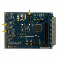
BOARD EVALUATION FOR AD7612
Manufacturer
Analog Devices Inc
Series
PulSAR®r
Specifications of EVAL-AD7612CBZ
Number Of Adc's
1
Number Of Bits
16
Sampling Rate (per Second)
750k
Data Interface
Serial, Parallel
Inputs Per Adc
1 Single Ended
Input Range
±5 V, ±10 V
Power (typ) @ Conditions
205mW @ 750kSPS
Voltage Supply Source
Analog and Digital
Operating Temperature
-40°C ~ 85°C
Utilized Ic / Part
AD7612
Lead Free Status / RoHS Status
Lead free / RoHS Compliant


AD7612
Internal Reference (REF = 5 V)
(PDREF = Low, PDBUF = Low)
To use the internal reference, the PDREF and PDBUF inputs
must be low. This enables the on-chip band gap reference, buffer,
and TEMP sensor resulting in a 5.00 V reference on the REF pin.
The internal reference is temperature-compensated to 5.000 V
±35 mV. The reference is trimmed to provide a typical drift of
3 ppm/°C. This typical drift characteristic is shown in Figure 19.
External 2.5 V Reference and Internal Buffer (REF = 5 V)
(PDREF = High, PDBUF = Low)
To use an external reference with the internal buffer, PDREF
should be high and PDBUF should be low. This powers down
the internal reference and allows the 2.5 V reference to be applied
to REFBUFIN producing 5 V on the REF pin. The internal ref-
erence buffer is useful in multiconverter applications since a
buffer is typically required in these applications.
External 5 V Reference (PDREF = High, PDBUF = High)
To use an external reference directly on the REF pin, PDREF
and PDBUF should both be high. PDREF and PDBUF power
down the internal reference and the internal reference buffer,
respectively. For improved drift performance, an external ref-
erence such as the
Reference Decoupling
Whether using an internal or external reference, the AD7612
voltage reference input (REF) has a dynamic input impedance;
therefore, it should be driven by a low impedance source with
efficient decoupling between the REF and REFGND inputs. This
decoupling depends on the choice of the voltage reference, but
usually consists of a low ESR capacitor connected to REF and
REFGND with minimum parasitic inductance. A 22 μF (X5R,
1206 size) ceramic chip capacitor (or 47 μF tantalum capacitor)
is appropriate when using either the internal reference or the
ADR445/ADR435 external reference.
The placement of the reference decoupling is also important to
the performance of the AD7612. The decoupling capacitor should
be mounted on the same side as the ADC right at the REF pin
with a thick PCB trace. The REFGND should also connect to
the reference decoupling capacitor with the shortest distance
and to the analog ground plane with several vias.
For applications that use multiple AD7612 or other PulSAR
devices, it is more effective to use the internal reference buffer
to buffer the external 2.5 V reference voltage.
The voltage reference temperature coefficient (TC) directly impacts
full scale; therefore, in applications where full-scale accuracy
matters, care must be taken with the TC. For instance, a
±15 ppm/°C TC of the reference changes full-scale by ±1 LSB/°C.
ADR445
or
ADR435
is recommended.
Rev. 0 | Page 22 of 32
Temperature Sensor
The TEMP pin measures the temperature of the AD7612. To
improve the calibration accuracy over the temperature range, the
output of the TEMP pin is applied to one of the inputs of the
analog switch (such as ADG779), and the ADC itself is used to
measure its own temperature. This configuration is shown
in Figure 30.
POWER SUPPLIES
The AD7612 uses five sets of power supply pins:
•
•
•
•
•
Core Supplies
The AVDD and DVDD supply the AD7612 analog and digital
cores respectively. Sufficient decoupling of these supplies is
required consisting of at least a 10 μF capacitor and 100 nF on
each supply. The 100 nF capacitors should be placed as close as
possible to the AD7612. To reduce the number of supplies needed,
the DVDD can be supplied through a simple RC filter from the
analog supply, as shown in Figure 27.
High Voltage Supplies
The high voltage bipolar supplies, VCC and VEE are required
and must be at least 2 V larger than the maximum input, V
For example, if using the bipolar 10 V range, the supplies should
be ±12 V minimum. Sufficient decoupling of these supplies is
also required consisting of at least a 10 μF capacitor and 100 nF
on each supply. For unipolar operation, the VEE supply can be
grounded with some slight THD performance degradation.
Digital Output Supply
The OVDD supplies the digital outputs and allows direct interface
with any logic working between 2.3 V and 5.25 V. OVDD should
be set to the same level as the system interface. Sufficient decou-
pling is required consisting of at least a 10 μF capacitor and 100 nF
with the 100 nF placed as close as possible to the AD7612.
ANALOG INPUT
(UNIPOLAR)
AVDD: analog 5 V core supply
VCC: analog high voltage positive supply
VEE: high voltage negative supply
DVDD: digital 5 V core supply
OVDD: digital input/output interface supply
ADG779
Figure 30. Use of the Temperature Sensor
AD8021
C
C
IN+
TEMP
AD7612
TEMPERATURE
SENSOR
IN
.
Related parts for EVAL-AD7612CBZ
Image
Part Number
Description
Manufacturer
Datasheet
Request
R


Part Number:
Description:
BOARD EVAL FOR SI270X-A
Manufacturer:
Silicon Laboratories Inc
Datasheet:

Part Number:
Description:
BUCK CONV REF DESIGN KIT IP1201
Manufacturer:
International Rectifier
Datasheet:
Part Number:
Description:
BOARD DEMO SYNC DUAL BUCK CNVTER
Manufacturer:
International Rectifier
Datasheet:
Part Number:
Description:
BOARD DEMO SYNC BUCK CONVETER
Manufacturer:
International Rectifier
Datasheet:

Part Number:
Description:
EVALBOARD/EB Omnidirectional microphone - Analog
Manufacturer:
Analog Devices
Datasheet:
Part Number:
Description:
EVALBOARD/EB Omnidirectional microphone - Analog
Manufacturer:
Analog Devices
Datasheet:


Part Number:
Description:
BOARD EVAL LED DRIVER LT3756
Manufacturer:
Linear Technology
Datasheet:

Part Number:
Description:
BOARD EVAL FOR AD7741/7742
Manufacturer:
Analog Devices Inc
Datasheet:

Part Number:
Description:
±1.7g Dual-Axis IMEMS Accelerometer Evaluation Board
Manufacturer:
Analog Devices Inc
Datasheet:

Part Number:
Description:
IC MULTIPLIER ANALOG 8-SOIC T/R
Manufacturer:
Analog Devices Inc
Datasheet:

Part Number:
Description:
IC ANALOG MULTIPLIER 8-DIP
Manufacturer:
Analog Devices Inc
Datasheet:
Part Number:
Description:
IC ANALOG MULTIPLIER 8-SOIC
Manufacturer:
Analog Devices Inc
Datasheet:
Part Number:
Description:
IC ANALOG MULTIPLIER 8-DIP
Manufacturer:
Analog Devices Inc
Datasheet: