EVAL-AD7612CBZ Analog Devices Inc, EVAL-AD7612CBZ Datasheet - Page 21
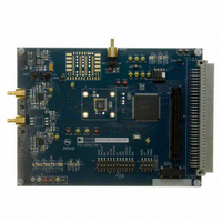
EVAL-AD7612CBZ
Manufacturer Part Number
EVAL-AD7612CBZ
Description
BOARD EVALUATION FOR AD7612
Manufacturer
Analog Devices Inc
Series
PulSAR®r
Specifications of EVAL-AD7612CBZ
Number Of Adc's
1
Number Of Bits
16
Sampling Rate (per Second)
750k
Data Interface
Serial, Parallel
Inputs Per Adc
1 Single Ended
Input Range
±5 V, ±10 V
Power (typ) @ Conditions
205mW @ 750kSPS
Voltage Supply Source
Analog and Digital
Operating Temperature
-40°C ~ 85°C
Utilized Ic / Part
AD7612
Lead Free Status / RoHS Status
Lead free / RoHS Compliant


DRIVER AMPLIFIER CHOICE
Although the AD7612 is easy to drive, the driver amplifier must
meet the following requirements:
•
•
•
For multichannel, multiplexed applications, the driver
amplifier and the AD7612 analog input circuit must be
able to settle for a full-scale step of the capacitor array at
a 16-bit level (0.0015%). For the amplifier, settling at 0.1%
to 0.01% is more commonly specified. This differs signifi-
cantly from the settling time at a 16-bit level and should
be verified prior to driver selection. The
combines ultra-low noise and high gain bandwidth and
meets this settling time requirement even when used with
gains of up to 13.
The noise generated by the driver amplifier needs to be
kept as low as possible to preserve the SNR and transition
noise performance of the AD7612. The noise coming from
the driver is filtered by the external 1-pole low-pass filter
as shown in Figure 27. The SNR degradation due to the
amplifier is
where:
V
f
N is the noise factor of the amplifier (+1 in buffer
configuration).
e
The driver needs to have a THD performance suitable to
that of the AD7612. Figure 15 shows the THD vs. frequency
that the driver should exceed.
V
amp, in nV/√Hz.
SNR
–3dB
N
NADC
NADC
is the equivalent input voltage noise density of the op
is the cutoff frequency of the input filter (3.9 MHz).
LOSS
is the noise of the ADC, which is:
=
=
10
V
2
20
INp-p
SNR
20
2
log
⎛
⎜
⎜
⎜
⎜ ⎜
⎝
V
NADC
2
V
+
NADC
π
2
f
−
3
dB
(
Ne
N
AD8021
)
2
⎞
⎟
⎟
⎟
⎟ ⎟
⎠
op amp
Rev. 0 | Page 21 of 32
The AD8021 meets these requirements and is appropriate for
almost all applications. The AD8021 needs a 10 pF external
compensation capacitor that should have good linearity as an
NPO ceramic or mica type. Moreover, the use of a noninverting
+1 gain arrangement is recommended and helps to obtain the
best signal-to-noise ratio.
The
and a gain of 1 is present. The
cations where high frequency (above 100 kHz) performance is not
required. In applications with a gain of 1, an 82 pF compensation
capacitor is required. The
current is needed in low frequency applications.
Since the AD7612 uses a large geometry, high voltage input
switch, the best linearity performance is obtained when using
the amplifier at its maximum full power bandwidth. Gaining
the amplifier to make use of the more dynamic range of the
ADC results in increased linearity errors. For applications
requiring more resolution, the use of an additional amplifier
with gain should precede a unity follower driving the AD7612.
See Table 8 for a list of recommended op amps.
Table 8. Recommended Driver Amplifiers
Amplifier
ADA4841-x
AD829
AD8021
AD8022
AD8610/AD8620
VOLTAGE REFERENCE INPUT/OUTPUT
The AD7612 allows the choice of either a very low temperature
drift internal voltage reference, an external reference or an external
buffered reference.
The internal reference of the AD7612 provides excellent perfor-
mance and can be used in almost all applications. However, the
linearity performance is guaranteed only with an external reference.
AD8022
can also be used when a dual version is needed
Typical Application
12 V supply, very low noise, low distortion,
low power, low frequency
±15 V supplies, very low noise, low frequency
±12 V supplies, very low noise, high frequency
±12 V supplies, very low noise, high
frequency, dual
±13 V supplies, low bias current, low
frequency, single/dual
AD8610
AD829
is an option when low bias
is an alternative in appli-
AD7612
Related parts for EVAL-AD7612CBZ
Image
Part Number
Description
Manufacturer
Datasheet
Request
R


Part Number:
Description:
BOARD EVAL FOR SI270X-A
Manufacturer:
Silicon Laboratories Inc
Datasheet:

Part Number:
Description:
BUCK CONV REF DESIGN KIT IP1201
Manufacturer:
International Rectifier
Datasheet:
Part Number:
Description:
BOARD DEMO SYNC DUAL BUCK CNVTER
Manufacturer:
International Rectifier
Datasheet:
Part Number:
Description:
BOARD DEMO SYNC BUCK CONVETER
Manufacturer:
International Rectifier
Datasheet:

Part Number:
Description:
EVALBOARD/EB Omnidirectional microphone - Analog
Manufacturer:
Analog Devices
Datasheet:
Part Number:
Description:
EVALBOARD/EB Omnidirectional microphone - Analog
Manufacturer:
Analog Devices
Datasheet:


Part Number:
Description:
BOARD EVAL LED DRIVER LT3756
Manufacturer:
Linear Technology
Datasheet:

Part Number:
Description:
BOARD EVAL FOR AD7741/7742
Manufacturer:
Analog Devices Inc
Datasheet:

Part Number:
Description:
±1.7g Dual-Axis IMEMS Accelerometer Evaluation Board
Manufacturer:
Analog Devices Inc
Datasheet:

Part Number:
Description:
IC MULTIPLIER ANALOG 8-SOIC T/R
Manufacturer:
Analog Devices Inc
Datasheet:

Part Number:
Description:
IC ANALOG MULTIPLIER 8-DIP
Manufacturer:
Analog Devices Inc
Datasheet:
Part Number:
Description:
IC ANALOG MULTIPLIER 8-SOIC
Manufacturer:
Analog Devices Inc
Datasheet:
Part Number:
Description:
IC ANALOG MULTIPLIER 8-DIP
Manufacturer:
Analog Devices Inc
Datasheet: