CDB5534U Cirrus Logic Inc, CDB5534U Datasheet - Page 3
CDB5534U
Manufacturer Part Number
CDB5534U
Description
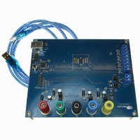
EVAL BOARD FOR CS5534
Manufacturer
Cirrus Logic Inc
Specifications of CDB5534U
Number Of Adc's
1
Number Of Bits
24
Sampling Rate (per Second)
3.84k
Data Interface
Serial
Inputs Per Adc
2 Single
Input Range
0 ~ 2.5 V
Power (typ) @ Conditions
35mW @ 5 V
Voltage Supply Source
Analog and Digital, Dual ±
Operating Temperature
-40°C ~ 85°C
Utilized Ic / Part
CS5534
Description/function
Audio DSPs
Operating Supply Voltage
5 V
Product
Audio Modules
For Use With/related Products
C8051F320
Lead Free Status / RoHS Status
Contains lead / RoHS non-compliant
Lead Free Status / RoHS Status
Lead free / RoHS Compliant, Contains lead / RoHS non-compliant
Other names
598-1016


1. HARDWARE
1.1
The CDB5534U evaluation board provides a quick means of evaluating the CS5534 Analog-to-Digital
Converter (ADC). The CS5534 is a highly integrated ∆Σ ADC which uses charge-balance techniques to
achieve 24-bit performance. The CS5534 includes a very low noise chopper-stabilized instrumentation
amplifier (6 nV/sqrt(Hz) @ 0.1 Hz) with selectable gains of 1×, 2×, 4×, 8×, 16×, 32×, and 64×. This ADC
also includes a fourth order ∆Σ modulator followed by a digital filter which provides twenty selectable out-
put word rates of 6.25 Hz, 7.5 Hz, 12.5 Hz, 15 Hz, 25 Hz, 30 Hz, 50 Hz, 60 Hz, 100 Hz, 120 Hz, 200 Hz,
240 Hz, 400 Hz, 480 Hz, 800 Hz, 960 Hz, 1.6 kHz, 1.92 kHz, 3.2 kHz and 3.84 kHz (XIN = 4.9152 MHz).
The CDB5534U is shipped with a CS5534 device soldered at U2. However, the CS5531, CS5532, or
CS5533 can be soldered in this same location. The CDB5534U software supports all four devices.
1.2
The CDB5534U evaluation board is partitioned into two main sections: analog and digital. The analog sec-
tion consists of the CS5534 and a precision voltage reference. The digital section consists of the micro-
controller, the reset circuitry, and the USB interface. The board also has power supply connections which
accommodate all of the various supply options of the CS5534.
The evaluation board’s analog section operates from either a single +5 V, dual ±2.5 V, or dual ±3 V power
supply. The evaluation board interfaces the CS5534 to an IBM
accomplish this, the board comes equipped with a microcontroller and a USB cable which physically in-
terfaces the evaluation board to the PC. The software provides easy access to the internal registers of the
CS5534, and provides a means to display and evaluate the performance of the ADC in the time domain
or the frequency domain.
1.2.1
The CS5534 is a high precision ∆Σ converter designed to accurately measure up to four fully-differential
analog voltage inputs while operating from a 4.9152 MHz crystal.
The evaluation board provides separate screw terminals to connect signals to each of the four input chan-
nels. The input screw terminals are labeled as AIN1 through AIN4, which correspond to physical input
channels 1 through 4 respectively. A simple RC network on each channel filters the sensor’s output to
reduce any interference picked up by the input leads. The 3 dB corner of the filter is approximately 52 kHz
differential and 56 kHz common mode. Figure 1 illustrates the schematic of the analog section.
The evaluation board provides three voltage reference options for VREF+ and VREF-. The three refer-
ence options for VREF+ include: VA+, the on-board LT1019 voltage reference, and external input (J12).
Table 1 illustrates the options available. With the J17 jumper in position VA+, the reference is supplied by
the VA+ analog supply. With the J17 jumper in position LT1019, the LT1019 provides a +2.5 V reference
(the LT1019 was chosen for its low drift, typically 5ppm/°C). By setting the J17 jumper to position VREF+,
the user can supply an external voltage reference to J12’s VREF+ input.
The three reference options for VREF- include: VA-, GND, and external input (J12). Table 2 illustrates the
options available. With the J18 jumper in position VA-, the reference is supplied by the VA- analog supply.
With the J18 jumper in position GND, the VREF- pin is connected to the board ground. By setting the J18
jumper to position VREF-, the user can supply an external voltage reference to J12’s VREF- input.
DS289DB6
Introduction
Evaluation Board Overview
Analog Section
®
compatible PC with a USB interface. To
CDB5534U
3
Related parts for CDB5534U
Image
Part Number
Description
Manufacturer
Datasheet
Request
R

Part Number:
Description:
Development Kit
Manufacturer:
Cirrus Logic Inc
Datasheet:
Part Number:
Description:
Development Kit
Manufacturer:
Cirrus Logic Inc
Datasheet:


Part Number:
Description:
High-efficiency PFC + Fluorescent Lamp Driver Reference Design
Manufacturer:
Cirrus Logic Inc
Datasheet:
Part Number:
Description:
Development Kit
Manufacturer:
Cirrus Logic Inc
Datasheet:
Part Number:
Description:
Development Kit
Manufacturer:
Cirrus Logic Inc
Datasheet:

Part Number:
Description:
Development Kit
Manufacturer:
Cirrus Logic Inc
Datasheet:
Part Number:
Description:
Development Kit
Manufacturer:
Cirrus Logic Inc
Datasheet:
Part Number:
Description:
Development Kit
Manufacturer:
Cirrus Logic Inc
Datasheet:
Part Number:
Description:
Development Kit
Manufacturer:
Cirrus Logic Inc
Datasheet:

Part Number:
Description:
EVALUATION BOARD FOR CS8427
Manufacturer:
Cirrus Logic Inc
Datasheet:

Part Number:
Description:
BOARD EVAL FOR CS8416 RCVR
Manufacturer:
Cirrus Logic Inc
Datasheet:

Part Number:
Description:
EVALUATION BOARD FOR CS8420
Manufacturer:
Cirrus Logic Inc
Datasheet:

Part Number:
Description:
KIT DEVELOPMENT EP9315 ARM9
Manufacturer:
Cirrus Logic Inc
Datasheet:

Part Number:
Description:
KIT DEVELOPMENT EP9302 ARM9
Manufacturer:
Cirrus Logic Inc
Datasheet: