M52221DEMO Freescale Semiconductor, M52221DEMO Datasheet - Page 24
M52221DEMO
Manufacturer Part Number
M52221DEMO
Description
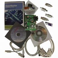
BOARD DEMO FOR MCF52221
Manufacturer
Freescale Semiconductor
Series
ColdFire®r
Type
MPUr
Datasheet
1.M52221DEMO.pdf
(56 pages)
Specifications of M52221DEMO
Contents
SBC, Cables and Software
Processor To Be Evaluated
MCF52221
Data Bus Width
32 bit
Interface Type
RS-232, USB
Silicon Manufacturer
Freescale
Core Architecture
Coldfire
Core Sub-architecture
Coldfire V2
Silicon Core Number
MCF52
Silicon Family Name
MCF5222x
Rohs Compliant
Yes
For Use With/related Products
MCF52221
Lead Free Status / RoHS Status
Lead free / RoHS Compliant


MCF52223 Family Configurations
1.13
Table 13
1.14
Table 14
1.15
These signals are used as the interface to the on-chip JTAG controller and the BDM logic.
24
General Purpose Timer
PWM Output Channels
Signal Name
Development Serial
Input/Output
Test Mode Select
Test Data Output
Test Data Input
describes the general purpose timer signals.
describes the PWM signals.
Signal Name
JTAG Enable
Signal Name
Breakpoint
Test Reset
Test Clock
General Purpose Timer Signals
Pulse Width Modulator Signals
Debug Support Signals
Clock
Abbreviation
Abbreviation
Abbreviation
GPT[3:0]
PWM[7:0]
JTAG_EN
DSCLK
TRST
TCLK
BKPT
TDO
TMS
TDI
MCF52223 ColdFire Microcontroller, Rev. 2
Table 15. Debug Support Signals
Pulse width modulated output for PWM channels.
Inputs to or outputs from the general purpose timer module.
Select between debug module and JTAG signals at reset.
This active-low signal is used to initialize the JTAG logic
asynchronously.
Used to synchronize the JTAG logic.
Used to sequence the JTAG state machine. TMS is sampled on the
rising edge of TCLK.
Serial input for test instructions and data. TDI is sampled on the rising
edge of TCLK.
Serial output for test instructions and data. TDO is tri-stateable and is
actively driven in the shift-IR and shift-DR controller states. TDO
changes on the falling edge of TCLK.
Development Serial Clock - Internally synchronized input. (The logic
level on DSCLK is validated if it has the same value on two
consecutive rising bus clock edges.) Clocks the serial communication
port to the debug module during packet transfers. Maximum frequency
is PSTCLK/5. At the synchronized rising edge of DSCLK, the data
input on DSI is sampled and DSO changes state.
Breakpoint - Input used to request a manual breakpoint. Assertion of
BKPT puts the processor into a halted state after the current
instruction completes. Halt status is reflected on processor
status/debug data signals (PST[3:0] and PSTDDATA[7:0]) as the
value 0xF. If CSR[BKD] is set (disabling normal BKPT functionality),
asserting BKPT generates a debug interrupt exception in the
processor.
Table 14. PWM Signals
Table 13. GPT Signals
Function
Function
Function
Freescale Semiconductor
I/O
I/O
O
O
I
I
I
I
I
I
I
I/O
I/O
Related parts for M52221DEMO
Image
Part Number
Description
Manufacturer
Datasheet
Request
R

Part Number:
Description:
Manufacturer:
Freescale Semiconductor, Inc
Datasheet:
Part Number:
Description:
Manufacturer:
Freescale Semiconductor, Inc
Datasheet:
Part Number:
Description:
Manufacturer:
Freescale Semiconductor, Inc
Datasheet:
Part Number:
Description:
Manufacturer:
Freescale Semiconductor, Inc
Datasheet:
Part Number:
Description:
Manufacturer:
Freescale Semiconductor, Inc
Datasheet:
Part Number:
Description:
Manufacturer:
Freescale Semiconductor, Inc
Datasheet:
Part Number:
Description:
Manufacturer:
Freescale Semiconductor, Inc
Datasheet:
Part Number:
Description:
Manufacturer:
Freescale Semiconductor, Inc
Datasheet:
Part Number:
Description:
Manufacturer:
Freescale Semiconductor, Inc
Datasheet:
Part Number:
Description:
Manufacturer:
Freescale Semiconductor, Inc
Datasheet:
Part Number:
Description:
Manufacturer:
Freescale Semiconductor, Inc
Datasheet:
Part Number:
Description:
Manufacturer:
Freescale Semiconductor, Inc
Datasheet:
Part Number:
Description:
Manufacturer:
Freescale Semiconductor, Inc
Datasheet:
Part Number:
Description:
Manufacturer:
Freescale Semiconductor, Inc
Datasheet:
Part Number:
Description:
Manufacturer:
Freescale Semiconductor, Inc
Datasheet: