M52221DEMO Freescale Semiconductor, M52221DEMO Datasheet - Page 34
M52221DEMO
Manufacturer Part Number
M52221DEMO
Description
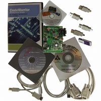
BOARD DEMO FOR MCF52221
Manufacturer
Freescale Semiconductor
Series
ColdFire®r
Type
MPUr
Datasheet
1.M52221DEMO.pdf
(56 pages)
Specifications of M52221DEMO
Contents
SBC, Cables and Software
Processor To Be Evaluated
MCF52221
Data Bus Width
32 bit
Interface Type
RS-232, USB
Silicon Manufacturer
Freescale
Core Architecture
Coldfire
Core Sub-architecture
Coldfire V2
Silicon Core Number
MCF52
Silicon Family Name
MCF5222x
Rohs Compliant
Yes
For Use With/related Products
MCF52221
Lead Free Status / RoHS Status
Lead free / RoHS Compliant


Electrical Characteristics
1
2
3
4
5
6
7
8
9
2.8
GPIO can be configured for certain pins of the QSPI, DDR Control, timer, UART, Interrupt
GPIO mode, the timing specification for these pins is given in
The GPIO timing is met under the following load test conditions:
34
Frequency un-LOCK range
Frequency LOCK range
CLKOUT period jitter
On-chip oscillator frequency
• Peak-to-peak (clock edge to clock edge)
• Long term (averaged over 2 ms interval)
All internal registers retain data at 0 Hz.
Depending on packaging; see
Loss of Reference Frequency is the reference frequency detected internally, which transitions the PLL into self clocked mode.
Self clocked mode frequency is the frequency at which the PLL operates when the reference frequency falls below f
default MFD/RFD settings.
This parameter is characterized before qualification rather than 100% tested.
Proper PC board layout procedures must be followed to achieve specifications.
This specification applies to the period required for the PLL to relock after changing the MFD frequency control bits in the
synthesizer control register (SYNCR).
Jitter is the average deviation from the programmed frequency measured over the specified interval at maximum f
Measurements are made with the device powered by filtered supplies and clocked by a stable external clock signal. Noise
injected into the PLL circuitry via V
for a given interval.
Based on slow system clock of 40 MHz measured at f
NUM
G1
G2
G3
G4
•
•
50 pF / 50 Ω for high drive
25 pF / 25 Ω for low drive
General Purpose I/O Timing
4, 5, 8 ,9
CLKOUT High to GPIO Output Invalid
CLKOUT High to GPIO Output Valid
CLKOUT High to GPIO Input Invalid
GPIO Input Valid to CLKOUT High
Characteristic
, measured at f
Table
Table 27. PLL Electrical Specifications (continued)
Characteristic
DDPLL
(V
.
DD
MCF52223 ColdFire Microcontroller, Rev. 2
and V
and V
SYS
Max
SSPLL
DDPLL
Table 28. GPIO Timing
and variation in crystal oscillator frequency increase the C
= 2.7 to 3.6 V, V
sys
max.
Table 28
SS
Symbol
and
C
f
f
= V
f
LCK
oco
UL
jitter
Symbol
t
Figure
t
CHPOV
t
CHPOI
t
SSPLL
PVCH
CHPI
= 0 V)
6.
–0.75
–1.5
7.84
Min
—
—
Min
1.5
1.5
—
and USB
9
Freescale Semiconductor
Max
0.75
8.16
interfaces. When in
1.5
.01
10
Max
10
—
—
—
jitter
percentage
sys
% f
LOR
% f
% f
MHz
Unit
.
Unit
sys
ns
ns
ns
ns
ref
ref
with
Related parts for M52221DEMO
Image
Part Number
Description
Manufacturer
Datasheet
Request
R

Part Number:
Description:
Manufacturer:
Freescale Semiconductor, Inc
Datasheet:
Part Number:
Description:
Manufacturer:
Freescale Semiconductor, Inc
Datasheet:
Part Number:
Description:
Manufacturer:
Freescale Semiconductor, Inc
Datasheet:
Part Number:
Description:
Manufacturer:
Freescale Semiconductor, Inc
Datasheet:
Part Number:
Description:
Manufacturer:
Freescale Semiconductor, Inc
Datasheet:
Part Number:
Description:
Manufacturer:
Freescale Semiconductor, Inc
Datasheet:
Part Number:
Description:
Manufacturer:
Freescale Semiconductor, Inc
Datasheet:
Part Number:
Description:
Manufacturer:
Freescale Semiconductor, Inc
Datasheet:
Part Number:
Description:
Manufacturer:
Freescale Semiconductor, Inc
Datasheet:
Part Number:
Description:
Manufacturer:
Freescale Semiconductor, Inc
Datasheet:
Part Number:
Description:
Manufacturer:
Freescale Semiconductor, Inc
Datasheet:
Part Number:
Description:
Manufacturer:
Freescale Semiconductor, Inc
Datasheet:
Part Number:
Description:
Manufacturer:
Freescale Semiconductor, Inc
Datasheet:
Part Number:
Description:
Manufacturer:
Freescale Semiconductor, Inc
Datasheet:
Part Number:
Description:
Manufacturer:
Freescale Semiconductor, Inc
Datasheet: