MPC566EVB Freescale Semiconductor, MPC566EVB Datasheet - Page 16
MPC566EVB
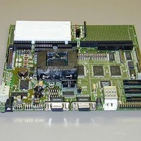
Manufacturer Part Number
MPC566EVB
Description
KIT EVALUATION FOR MPC565/566
Manufacturer
Freescale Semiconductor
Specifications of MPC566EVB
Processor To Be Evaluated
MPC56x
Data Bus Width
32 bit
Interface Type
RS-232, Ethernet
Lead Free Status / RoHS Status
Contains lead / RoHS non-compliant


System Memory
Following is the default memory map for this board as configured by the Debug Monitor located
in the external flash bank. The internal memory space of the MPC566 is detailed further in the
MPC565-6 Users Manual. Chip Selects 0-3 can be changed by user software to map the external
memory in different locations but the chip select configuration such as wait states and transfer
acknowledge for each memory type should be maintained.
Possible Chip Select usage:
Synchronous SRAM Memory Bank
Synchronous FLASH Memory Bank
10/100T / LCD Port
MPC566 Internal Flash
ory map of chip selects
The MPC566EVB Default Memory Map shows the MPC566EVB memory map.
1.2.5.1
The MPC566EVB board has one internal memory bank, two external memory banks and a
Peripheral memory bank that provide:
1-6
36KByte Internal SRAM
MPC566
256K x 32bit (1MByte) Synchronous Static RAM (U2/3).
Memory Device / Bank Selection and Configuration.
512K byte Internal FLASH Memory (U1)
0x0000_0000 - 0x0007_FFFF
0x0010_0000 - 0x002F_7FFF
0x002F_8000 - 0x002F_8FFF
0x002F_9000 - 0x002F_9FFF
0x002F_A000 - 0x002F_BFFF
0x002F_C000 - 0x002F_FFFF
0x0030_0000 - 0x0030_7FFF
0x0030_8000 - 0x0037_FFFF
0x0038_0000 - 0x0038_007F
0x0038_0080 - 0x0038_3FFF
0x0038_4000 - 0x003F_6FFF
0x003F_7000 - 0x003F_FFFF
0x0080_0000 - 0x00A0_0000
0x0100_0000 - 0x0108_0000
0xFFF0_0000 - 0xFFFF_FFFF
Table 1-1. The MPC566EVB Default Memory Map
Address Range
Freescale Semiconductor, Inc.
For More Information On This Product,
MPC566EVB User’s Manual
Go to: www.freescale.com
CS0 or CS1
CS0 or CS2
CS3
N/A
1MB UC3F Flash
Reserved for Flash
BBC DECRAM 4 KBytes
Reserved for BBC
BBC Control
USIU & Flash Control
UIMB I/F & IMB Modules 32KBytes
Reserved for IMB
CALRAM/READI Control
Reserved (L-bus Control)
Reserved (L-bus Memory)
CALRAM (internal SRAM)
External Flash 2MByte (0x0090_0000 -
0x00A0_0000 reserved for dBUG)
Ethernet
External SRAM 1MB
Signal and Device
default CS1, MAP SW. 1,2
default CS0, MAP SW. 3,4
default CS3, MAP SW. 6,7
MAP_SW. 8, may effect mem-
Related parts for MPC566EVB
Image
Part Number
Description
Manufacturer
Datasheet
Request
R

Part Number:
Description:
Manufacturer:
Freescale Semiconductor, Inc
Datasheet:
Part Number:
Description:
Manufacturer:
Freescale Semiconductor, Inc
Datasheet:
Part Number:
Description:
Manufacturer:
Freescale Semiconductor, Inc
Datasheet:
Part Number:
Description:
Manufacturer:
Freescale Semiconductor, Inc
Datasheet:
Part Number:
Description:
Manufacturer:
Freescale Semiconductor, Inc
Datasheet:
Part Number:
Description:
Manufacturer:
Freescale Semiconductor, Inc
Datasheet:
Part Number:
Description:
Manufacturer:
Freescale Semiconductor, Inc
Datasheet:
Part Number:
Description:
Manufacturer:
Freescale Semiconductor, Inc
Datasheet:
Part Number:
Description:
Manufacturer:
Freescale Semiconductor, Inc
Datasheet:
Part Number:
Description:
Manufacturer:
Freescale Semiconductor, Inc
Datasheet:
Part Number:
Description:
Manufacturer:
Freescale Semiconductor, Inc
Datasheet:
Part Number:
Description:
Manufacturer:
Freescale Semiconductor, Inc
Datasheet:
Part Number:
Description:
Manufacturer:
Freescale Semiconductor, Inc
Datasheet:
Part Number:
Description:
Manufacturer:
Freescale Semiconductor, Inc
Datasheet:
Part Number:
Description:
Manufacturer:
Freescale Semiconductor, Inc
Datasheet: