MPC566EVB Freescale Semiconductor, MPC566EVB Datasheet - Page 17
MPC566EVB
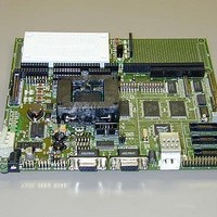
Manufacturer Part Number
MPC566EVB
Description
KIT EVALUATION FOR MPC565/566
Manufacturer
Freescale Semiconductor
Specifications of MPC566EVB
Processor To Be Evaluated
MPC56x
Data Bus Width
32 bit
Interface Type
RS-232, Ethernet
Lead Free Status / RoHS Status
Contains lead / RoHS non-compliant


Each external RAM or Flash memory bank can be configured individually to operate from the
MPC566 chip selects. Caution should be used not to place more than one memory bank on the CS0
chip select and to properly configure the chip select to control the memory devices provided in the
memory bank correctly. Failure to observe precautions may render the external memory bus
inoperable.
The MAP Switch (MAP_SW) connects MPC566 chip selects to the different external memory
banks. If memory access problems occur, the settings of these options and the associated chip
select configurations should be reviewed with some detail. Information to configure the chip
selects and memory is detailed in the following section.
1.2.5.2
Application software that executes on Reset must configure each memory bank chip select
properly for correct operation. Chip Select Memory Options shows the default memory settings
programmed by the dBUG ROM monitor and may be applied for most user applications:
1.2.5.3 Reset Vector Mapping
After reset, the processor attempts to execute at physical address 0x0000_0100 if the hard reset
configuration word IP bit is cleared to 0 or physical address 0xFFF0_0100 if the hard reset
configuration word IP bit is set to 1. This requires the board to have a non-volatile memory device
in this range with the correct information stored in it. The MPC566 processor chip-select zero
(CS0) responds to any accesses after reset until the OR0 is written. Since CS0 (the global chip
select) is connected to the Flash ROM (U6), the Flash ROM initially appears at address
0xFFF0_0000. The initialization routine then programs the chip-select logic, locates the Flash
CS1 = SRAM
CS1 = SRAM, asynchro-
nous access mode
CS0 = FLASH
CS0 = FLASH, asynchro-
nous access mode
CS3 = Peripheral
CS3 = Peripheral, asyn-
chronous
512K x 32bit (2MByte) Synchronous Flash EEPROM (U4)
Peripherals 10/100T Ethernet and LCD Port
Memory Bank
Memory Bank Chip Select Configuration
Reg.
Freescale Semiconductor, Inc.
OR1
OR0
OR3
Table 1-2. Chip Select Memory Options
BR1
BR0
BR3
For More Information On This Product,
Default Value
0xFFF0_0000
0xFFE0_0030
0xFFFF_80F0
0xFFF0_0003
0x0080_0003
0x0100_0807
MPC566EVB User’s Manual
Go to: www.freescale.com
Base Address = 0xFFF0_0000, Port width = 32 bit *Default
Memory Range = 0xFFF0_0000 > 0xFFFF_FFFF, wait state
Base address 0x0080_0000, Port width = 32 bit *Default
Memory range = 0x0080_0000 > 0x009F_FFFF, wait state
= 3, asynchronous operation 40Mhz clock, 95ns device.
Note U4 = 2M bytes and will mirror 2x with this setting.
Usable range = 0x0080_0000 > 0x008F_FFFF (dBUG mon-
itor is in upper half starting at 0x0090_0000)
Base address = 0x0100_0000, Port width = 16 bit *Default
Memory Range 0x0100_0000 > 0100_7FFF, wait state =
External Terminate (TA*) *Default Note Peripheral memory
map.
= 0.
External TA* generation provided.
Notes
System Memory
1-7
Related parts for MPC566EVB
Image
Part Number
Description
Manufacturer
Datasheet
Request
R

Part Number:
Description:
Manufacturer:
Freescale Semiconductor, Inc
Datasheet:
Part Number:
Description:
Manufacturer:
Freescale Semiconductor, Inc
Datasheet:
Part Number:
Description:
Manufacturer:
Freescale Semiconductor, Inc
Datasheet:
Part Number:
Description:
Manufacturer:
Freescale Semiconductor, Inc
Datasheet:
Part Number:
Description:
Manufacturer:
Freescale Semiconductor, Inc
Datasheet:
Part Number:
Description:
Manufacturer:
Freescale Semiconductor, Inc
Datasheet:
Part Number:
Description:
Manufacturer:
Freescale Semiconductor, Inc
Datasheet:
Part Number:
Description:
Manufacturer:
Freescale Semiconductor, Inc
Datasheet:
Part Number:
Description:
Manufacturer:
Freescale Semiconductor, Inc
Datasheet:
Part Number:
Description:
Manufacturer:
Freescale Semiconductor, Inc
Datasheet:
Part Number:
Description:
Manufacturer:
Freescale Semiconductor, Inc
Datasheet:
Part Number:
Description:
Manufacturer:
Freescale Semiconductor, Inc
Datasheet:
Part Number:
Description:
Manufacturer:
Freescale Semiconductor, Inc
Datasheet:
Part Number:
Description:
Manufacturer:
Freescale Semiconductor, Inc
Datasheet:
Part Number:
Description:
Manufacturer:
Freescale Semiconductor, Inc
Datasheet: