MPC566EVB Freescale Semiconductor, MPC566EVB Datasheet - Page 19
MPC566EVB
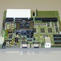
Manufacturer Part Number
MPC566EVB
Description
KIT EVALUATION FOR MPC565/566
Manufacturer
Freescale Semiconductor
Specifications of MPC566EVB
Processor To Be Evaluated
MPC56x
Data Bus Width
32 bit
Interface Type
RS-232, Ethernet
Lead Free Status / RoHS Status
Contains lead / RoHS non-compliant


Exception Vector Table in memory. Exceptions are handled in program order based on PowerPC
architecture requirements. When an exception occurs that was caused by an instruction, any
unexecuted instructions that appear earlier in the instruction stream are required to complete before
the exception is taken. Exceptions no associated with a specific instruction (asynchronous
exceptions) are recognized when they occur. Exception handlers should save the information in
SRR0 and SRR1 soon after the exception is taken to prevent this information from being lost due
to another exception being taken.
The processor goes to an exception routine via the exception table. This table is stored in the Flash
EEPROM. The address of the table location is set by the IP bit (switch 5 of MAP_SWITCH). The
dBUG ROM monitor writes a copy of the exception table into the RAM starting at 0xFFF0_0000.
To set an exception vector, the user places the address of the exception handler in the appropriate
vector in the vector table located at 0xFFF0_0000.
The MPC566’s interrupt controller supports up to 8 external interrups (0 - 7), eight levels for all
internal USIU interrupt sources and 32 levels for internal peripheral modules. It has an enhanced
mode of operation, which simplifies the MPC566 interrupt structure and speeds up interrupt
processing.
The MPC566EVB hardware uses IRQ[0]/SGPIOC[0] to support the ABORT (Non Maskable
Interrupt) function using the ABORT switch (SWITCH1 when BRK_EN jumper is inserted). This
switch is used to force a non-maskable interrupt if the user's program execution should be aborted
without issuing a RESET.
Refer to MPC566 User’s Manual for more information about the interrupt controller.
1.3.5 TA Generation
The TA signal is driven by the slave device from which the current transaction was addressed. It
indicates that the slave has received the data on the write cycle or returned data on the read cycle.
If the transaction is a burst, TA should be asserted for each one of the transaction beats. The
MPC566 drives TA when the slave device is controlled by the on-chip memory controller or when
an external master initiated a transaction to an internal slave module. TA is used to indicate the
completion of the bus cycle. It also allows devices with different access times to communicate with
the processor properly (i.e. asynchronously) like the Ethernet controller. The internal TA generator
is used for all external memories. External TA is only used for Ethernet/LCD.
1.3.6 User’s Program
Switch 5 on the MAP_SW bank of switches allows users to test code from boot/PORESET without
having to overwrite the ROM Monitor. The user’s code will boot from internal flash
(0x0000_0000) needs to contain the start of the Exception Vector Table).
When the switch is ON (IP is set), the behavior of the system is normal, dBUG boots and then runs
from 0x0090_0000.
Procedure:
No interrupt sources should have the same level and priority as
another. Programming two interrupt sources with the same level and
priority can result in undefined operation.
Freescale Semiconductor, Inc.
For More Information On This Product,
MPC566EVB User’s Manual
Go to: www.freescale.com
NOTE:
Support Logic
1-9
Related parts for MPC566EVB
Image
Part Number
Description
Manufacturer
Datasheet
Request
R

Part Number:
Description:
Manufacturer:
Freescale Semiconductor, Inc
Datasheet:
Part Number:
Description:
Manufacturer:
Freescale Semiconductor, Inc
Datasheet:
Part Number:
Description:
Manufacturer:
Freescale Semiconductor, Inc
Datasheet:
Part Number:
Description:
Manufacturer:
Freescale Semiconductor, Inc
Datasheet:
Part Number:
Description:
Manufacturer:
Freescale Semiconductor, Inc
Datasheet:
Part Number:
Description:
Manufacturer:
Freescale Semiconductor, Inc
Datasheet:
Part Number:
Description:
Manufacturer:
Freescale Semiconductor, Inc
Datasheet:
Part Number:
Description:
Manufacturer:
Freescale Semiconductor, Inc
Datasheet:
Part Number:
Description:
Manufacturer:
Freescale Semiconductor, Inc
Datasheet:
Part Number:
Description:
Manufacturer:
Freescale Semiconductor, Inc
Datasheet:
Part Number:
Description:
Manufacturer:
Freescale Semiconductor, Inc
Datasheet:
Part Number:
Description:
Manufacturer:
Freescale Semiconductor, Inc
Datasheet:
Part Number:
Description:
Manufacturer:
Freescale Semiconductor, Inc
Datasheet:
Part Number:
Description:
Manufacturer:
Freescale Semiconductor, Inc
Datasheet:
Part Number:
Description:
Manufacturer:
Freescale Semiconductor, Inc
Datasheet: