PESD1LIN,115 NXP Semiconductors, PESD1LIN,115 Datasheet
PESD1LIN,115
Specifications of PESD1LIN,115
934058897115
PESD1LIN T/R
PESD1LIN T/R
Available stocks


Related parts for PESD1LIN,115


PESD1LIN,115 Summary of contents
Page 1
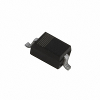
PESD1LIN LIN bus ESD protection diode Rev. 02 — 12 November 2008 1. Product profile 1.1 General description PESD1LIN in a very small SOD323 (SC-76) Surface-Mounted Device (SMD) plastic package designed to protect one automotive Local Interconnect Network (LIN) bus ...
Page 2
... NXP Semiconductors 2. Pinning information Table 2. Pin Ordering information Table 3. Type number Package PESD1LIN 4. Marking Table 4. Type number PESD1LIN 5. Limiting values Table 5. In accordance with the Absolute Maximum Rating System (IEC 60134). Symbol amb T stg [1] Non-repetitive current pulse 8/20 s exponential decay waveform according to IEC 61000-4-5. ...
Page 3
... NXP Semiconductors Table 6. Symbol V ESD [1] Device stressed with ten non-repetitive ESD pulses. Table 7. Standard IEC 61000-4-2; level 4 (ESD) MIL-STD-883; class 3 (human body model) 120 100 % (%) Fig 1. 8/20 s pulse waveform according to IEC 61000-4-5 PESD1LIN_2 Product data sheet ESD maximum ratings Parameter Conditions ...
Page 4
... NXP Semiconductors 6. Characteristics Table unless otherwise specified. amb Symbol V RWM dif [1] Non-repetitive current pulse 8/20 s exponential decay waveform according to IEC 61000-4- ( amb Fig 3. Peak pulse power as a function of exponential pulse duration; typical values PESD1LIN_2 Product data sheet Characteristics Parameter Conditions ...
Page 5
... NXP Semiconductors ESD TESTER IEC 61000-4-2 network C = 150 pF 330 Z Z GND unclamped 1 kV ESD voltage waveform (IEC 61000-4-2 network) GND unclamped 1 kV ESD voltage waveform (IEC 61000-4-2 network) Fig 5. ESD clamping test setup and waveforms PESD1LIN_2 Product data sheet RG 223/U 50 coax 450 D ...
Page 6
... NXP Semiconductors 7. Application information The PESD1LIN is designed for the protection of one LIN bus signal line from the damage caused by ESD and surge pulses. The PESD1LIN provides a surge capability 160 W per line for a 8/20 s waveform. Fig 6. Circuit board layout and protection device placement Circuit board layout is critical for the suppression of ESD, Electrical Fast Transient (EFT) and surge transients ...
Page 7
... NXP Semiconductors 8. Package outline Fig 7. 9. Packing information Table 9. The indicated -xxx are the last three digits of the 12NC ordering code. Type number Package Description PESD1LIN [1] For further information and the availability of packing methods, see PESD1LIN_2 Product data sheet 1.35 1.15 2 ...
Page 8
... NXP Semiconductors 10. Soldering 1.65 Fig 8. 2.75 Fig 9. PESD1LIN_2 Product data sheet 3.05 2.1 0.95 2 Reflow soldering footprint SOD323 (SC-76) 5 2 Wave soldering footprint SOD323 (SC-76) Rev. 02 — 12 November 2008 PESD1LIN LIN bus ESD protection diode solder lands solder resist ...
Page 9
... Document ID Release date PESD1LIN_2 20081112 • Modifications: The format of this data sheet has been redesigned to comply with the new identity guidelines of NXP Semiconductors. • Legal texts have been adapted to the new company name where appropriate. • Table voltage • Figure • ...
Page 10
... Right to make changes — NXP Semiconductors reserves the right to make changes to information published in this document, including without limitation specifications and product descriptions, at any time and without notice ...
Page 11
... NXP Semiconductors 14. Contents 1 Product profi 1.1 General description 1.2 Features . . . . . . . . . . . . . . . . . . . . . . . . . . . . . . 1 1.3 Applications . . . . . . . . . . . . . . . . . . . . . . . . . . . 1 1.4 Quick reference data Pinning information . . . . . . . . . . . . . . . . . . . . . . 2 3 Ordering information . . . . . . . . . . . . . . . . . . . . . 2 4 Marking . . . . . . . . . . . . . . . . . . . . . . . . . . . . . . . . 2 5 Limiting values Characteristics . . . . . . . . . . . . . . . . . . . . . . . . . . 4 7 Application information Package outline . . . . . . . . . . . . . . . . . . . . . . . . . 7 9 Packing information Soldering . . . . . . . . . . . . . . . . . . . . . . . . . . . . . . 8 11 Revision history . . . . . . . . . . . . . . . . . . . . . . . . . 9 12 Legal information ...