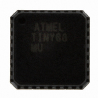
ATTINY88-MU Atmel, ATTINY88-MU Datasheet - Page 21

ATTINY88-MU
Manufacturer Part Number
ATTINY88-MU
Description
MCU AVR 8K ISP FLASH 1.8V 32-QFN
Manufacturer
Atmel
Series
AVR® ATtinyr
Specifications of ATTINY88-MU
Core Processor
AVR
Core Size
8-Bit
Speed
12MHz
Connectivity
I²C, SPI
Peripherals
Brown-out Detect/Reset, POR, WDT
Number Of I /o
28
Program Memory Size
8KB (4K x 16)
Program Memory Type
FLASH
Eeprom Size
64 x 8
Ram Size
512 x 8
Voltage - Supply (vcc/vdd)
1.8 V ~ 5.5 V
Data Converters
A/D 8x10b
Oscillator Type
Internal
Operating Temperature
-40°C ~ 85°C
Package / Case
32-VQFN Exposed Pad, 32-HVQFN, 32-SQFN, 32-DHVQFN
Processor Series
ATTINY8x
Core
AVR8
Data Bus Width
8 bit
Data Ram Size
512 B
Interface Type
2-Wire, I2S, SPI
Maximum Clock Frequency
12 MHz
Number Of Programmable I/os
28
Number Of Timers
2
Maximum Operating Temperature
+ 85 C
Mounting Style
SMD/SMT
3rd Party Development Tools
EWAVR, EWAVR-BL
Development Tools By Supplier
ATAVRDRAGON, ATSTK500, ATSTK600, ATAVRISP2, ATAVRONEKIT, ATQT600, ATAVRTS2080B
Minimum Operating Temperature
- 40 C
On-chip Adc
10 bit, 8 Channel
Package
32QFN EP
Device Core
AVR
Family Name
ATtiny
Maximum Speed
12 MHz
Operating Supply Voltage
2.5|3.3|5 V
Cpu Family
ATtiny
Device Core Size
8b
Frequency (max)
12MHz
Total Internal Ram Size
512Byte
# I/os (max)
28
Number Of Timers - General Purpose
2
Operating Supply Voltage (typ)
2.5/3.3/5V
Operating Supply Voltage (max)
5.5V
Operating Supply Voltage (min)
1.8V
Instruction Set Architecture
RISC
Operating Temp Range
-40C to 85C
Operating Temperature Classification
Industrial
Mounting
Surface Mount
Pin Count
32
Package Type
QFN EP
For Use With
ATSTK600-DIP40 - STK600 SOCKET/ADAPTER 40-PDIPATAVRDRAGON - KIT DRAGON 32KB FLASH MEM AVR
Lead Free Status / RoHS Status
Lead free / RoHS Compliant
Available stocks
Company
Part Number
Manufacturer
Quantity
Price
Company:
Part Number:
ATTINY88-MU
Manufacturer:
ATMEL
Quantity:
21 342
Part Number:
ATTINY88-MU
Manufacturer:
ATMEL/爱特梅尔
Quantity:
20 000
Part Number:
ATTINY88-MUR
Manufacturer:
AT
Quantity:
20 000
5.3.2
5.3.3
5.3.4
8008G–AVR–04/11
Read
Erase
Write
The programming method is selected using the EEPROM Programming Mode bits (EEPM1 and
EEPM0) in EEPROM Control Register (EECR). See
times are given in the same table.
Since EEPROM programming takes some time the application must wait for one operation to
complete before starting the next. This can be done by either polling the EEPROM Program
Enable bit (EEPE) in EEPROM Control Register (EECR), or via the EEPROM Ready Interrupt.
The EEPROM interrupt is controlled by the EEPROM Ready Interrupt Enable (EERIE) bit in
EECR.
To read an EEPROM memory location follow the procedure below:
In order to prevent unintentional EEPROM writes, a specific procedure must be followed to
erase memory locations. To erase an EEPROM memory location follow the procedure below:
The EEPE bit remains set until the erase operation has completed. While the device is busy pro-
gramming, it is not possible to perform any other EEPROM operations.
In order to prevent unintentional EEPROM writes, a specific procedure must be followed to write
to memory locations.
Before writing data to EEPROM the target location must be erased. This can be done either in
the same operation or as part of a split operation. Writing to an unerased EEPROM location will
result in corrupted data.
• Poll the EEPROM Program Enable bit (EEPE) in EEPROM Control Register (EECR) to make
• Write target address to EEPROM Address Registers (EEARH/EEARL).
• Start the read operation by setting the EEPROM Read Enable bit (EERE) in the EEPROM
• Read data from the EEPROM Data Register (EEDR).
• Poll the EEPROM Program Enable bit (EEPE) in EEPROM Control Register (EECR) to make
• Set mode of programming to erase by writing EEPROM Programming Mode bits (EEPM0
• Write target address to EEPROM Address Registers (EEARH/EEARL).
• Enable erase by setting EEPROM Master Program Enable (EEMPE) in EEPROM Control
before writing to them. This can be done at times when the system allows time-critical
operations, typically at start-up and initialisation.
sure no other EEPROM operations are in process. If set, wait to clear.
Control Register (EECR). During the read operation, the CPU is halted for four clock cycles
before executing the next instruction.
sure no other EEPROM operations are in process. If set, wait to clear.
and EEPM1) in EEPROM Control Register (EECR).
Register (EECR). Within four clock cycles, start the erase operation by setting the EEPROM
Program Enable bit (EEPE) in the EEPROM Control Register (EECR). During the erase
operation, the CPU is halted for two clock cycles before executing the next instruction.
Table 5-4 on page
ATtiny48/88
26. Write and erase
21


