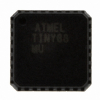
ATTINY88-MU Atmel, ATTINY88-MU Datasheet - Page 86

ATTINY88-MU
Manufacturer Part Number
ATTINY88-MU
Description
MCU AVR 8K ISP FLASH 1.8V 32-QFN
Manufacturer
Atmel
Series
AVR® ATtinyr
Specifications of ATTINY88-MU
Core Processor
AVR
Core Size
8-Bit
Speed
12MHz
Connectivity
I²C, SPI
Peripherals
Brown-out Detect/Reset, POR, WDT
Number Of I /o
28
Program Memory Size
8KB (4K x 16)
Program Memory Type
FLASH
Eeprom Size
64 x 8
Ram Size
512 x 8
Voltage - Supply (vcc/vdd)
1.8 V ~ 5.5 V
Data Converters
A/D 8x10b
Oscillator Type
Internal
Operating Temperature
-40°C ~ 85°C
Package / Case
32-VQFN Exposed Pad, 32-HVQFN, 32-SQFN, 32-DHVQFN
Processor Series
ATTINY8x
Core
AVR8
Data Bus Width
8 bit
Data Ram Size
512 B
Interface Type
2-Wire, I2S, SPI
Maximum Clock Frequency
12 MHz
Number Of Programmable I/os
28
Number Of Timers
2
Maximum Operating Temperature
+ 85 C
Mounting Style
SMD/SMT
3rd Party Development Tools
EWAVR, EWAVR-BL
Development Tools By Supplier
ATAVRDRAGON, ATSTK500, ATSTK600, ATAVRISP2, ATAVRONEKIT, ATQT600, ATAVRTS2080B
Minimum Operating Temperature
- 40 C
On-chip Adc
10 bit, 8 Channel
Package
32QFN EP
Device Core
AVR
Family Name
ATtiny
Maximum Speed
12 MHz
Operating Supply Voltage
2.5|3.3|5 V
Cpu Family
ATtiny
Device Core Size
8b
Frequency (max)
12MHz
Total Internal Ram Size
512Byte
# I/os (max)
28
Number Of Timers - General Purpose
2
Operating Supply Voltage (typ)
2.5/3.3/5V
Operating Supply Voltage (max)
5.5V
Operating Supply Voltage (min)
1.8V
Instruction Set Architecture
RISC
Operating Temp Range
-40C to 85C
Operating Temperature Classification
Industrial
Mounting
Surface Mount
Pin Count
32
Package Type
QFN EP
For Use With
ATSTK600-DIP40 - STK600 SOCKET/ADAPTER 40-PDIPATAVRDRAGON - KIT DRAGON 32KB FLASH MEM AVR
Lead Free Status / RoHS Status
Lead free / RoHS Compliant
Available stocks
Company
Part Number
Manufacturer
Quantity
Price
Company:
Part Number:
ATTINY88-MU
Manufacturer:
ATMEL
Quantity:
21 342
Part Number:
ATTINY88-MU
Manufacturer:
ATMEL/爱特梅尔
Quantity:
20 000
Part Number:
ATTINY88-MUR
Manufacturer:
AT
Quantity:
20 000
- Current page: 86 of 302
- Download datasheet (9Mb)
11.8.2
11.8.3
86
ATtiny48/88
TCNT0 – Timer/Counter Register
OCR0A – Output Compare Register A
Table 11-2.
Notes:
• Bits 2:0 – CS0[2:0]: Clock Select
The three Clock Select bits select the clock source to be used by the Timer/Counter.
Table 11-3.
If external pin modes are used for the Timer/Counter0, transitions on the T0 pin will clock the
counter even if the pin is configured as an output. This feature allows software control of the
counting.
The Timer/Counter Register gives direct access, both for read and write operations, to the
Timer/Counter unit 8-bit counter. Writing to the TCNT0 Register blocks (removes) the Compare
Match on the following timer clock. Modifying the counter (TCNT0) while the counter is running,
introduces a risk of missing a Compare Match between TCNT0 and the OCR0x Registers.
The Output Compare Register A contains an 8-bit value that is continuously compared with the
counter value (TCNT0). A match can be used to generate an Output Compare interrupt.
Bit
0x26 (0x46)
Read/Write
Initial Value
Bit
0x27 (0x47)
Read/Write
Initial Value
CS02
Mode
0
0
0
0
1
1
1
1
0
1
1. MAX
CS01
0
0
1
1
0
0
1
1
CTC Mode Bit Description
Clock Select Bit Description
R/W
R/W
CTC0
7
0
7
0
0
1
CS00
= 0xFF
0
1
0
1
0
1
0
1
R/W
R/W
6
0
6
0
Timer/Counter
Mode of Operation
Normal
CTC
Description
No clock source (Timer/Counter stopped)
clk
clk
clk
clk
clk
External clock source on T0 pin. Clock on falling edge.
External clock source on T0 pin. Clock on rising edge.
I/O
I/O
I/O
I/O
I/O
/8 (From prescaler)
/64 (From prescaler)
/256 (From prescaler)
/1024 (From prescaler)
(No prescaling)
R/W
R/W
5
0
5
0
R/W
R/W
4
0
4
0
OCR0A[7:0]
TCNT0[7:0]
OCRA
0xFF
TOP
R/W
R/W
3
0
3
0
R/W
R/W
2
0
2
0
Update of
Immediate
Immediate
OCRx at
R/W
R/W
1
0
1
0
R/W
R/W
TOV Flag
0
0
0
0
Set on
8008G–AVR–04/11
MAX
MAX
(1)
OCR0A
TCNT0
Related parts for ATTINY88-MU
Image
Part Number
Description
Manufacturer
Datasheet
Request
R

Part Number:
Description:
IC, MCU, 8BIT, 2K FLASH, 20SOIC
Manufacturer:
Atmel
Datasheet:

Part Number:
Description:
IC, MCU, 8BIT, 2K FLASH, 20PDIP
Manufacturer:
Atmel
Datasheet:

Part Number:
Description:
IC, MCU, 8BIT, 8K FLASH, 20PDIP
Manufacturer:
Atmel
Datasheet:

Part Number:
Description:
IC, MCU, 8BIT, 8K FLASH, 20SOIC
Manufacturer:
Atmel
Datasheet:

Part Number:
Description:
DEV KIT FOR AVR/AVR32
Manufacturer:
Atmel
Datasheet:

Part Number:
Description:
INTERVAL AND WIPE/WASH WIPER CONTROL IC WITH DELAY
Manufacturer:
ATMEL Corporation
Datasheet:

Part Number:
Description:
Low-Voltage Voice-Switched IC for Hands-Free Operation
Manufacturer:
ATMEL Corporation
Datasheet:

Part Number:
Description:
MONOLITHIC INTEGRATED FEATUREPHONE CIRCUIT
Manufacturer:
ATMEL Corporation
Datasheet:

Part Number:
Description:
AM-FM Receiver IC U4255BM-M
Manufacturer:
ATMEL Corporation
Datasheet:

Part Number:
Description:
Monolithic Integrated Feature Phone Circuit
Manufacturer:
ATMEL Corporation
Datasheet:

Part Number:
Description:
Multistandard Video-IF and Quasi Parallel Sound Processing
Manufacturer:
ATMEL Corporation
Datasheet:

Part Number:
Description:
High-performance EE PLD
Manufacturer:
ATMEL Corporation
Datasheet:


