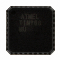
ATTINY88-MU Atmel, ATTINY88-MU Datasheet - Page 57

ATTINY88-MU
Manufacturer Part Number
ATTINY88-MU
Description
MCU AVR 8K ISP FLASH 1.8V 32-QFN
Manufacturer
Atmel
Series
AVR® ATtinyr
Specifications of ATTINY88-MU
Core Processor
AVR
Core Size
8-Bit
Speed
12MHz
Connectivity
I²C, SPI
Peripherals
Brown-out Detect/Reset, POR, WDT
Number Of I /o
28
Program Memory Size
8KB (4K x 16)
Program Memory Type
FLASH
Eeprom Size
64 x 8
Ram Size
512 x 8
Voltage - Supply (vcc/vdd)
1.8 V ~ 5.5 V
Data Converters
A/D 8x10b
Oscillator Type
Internal
Operating Temperature
-40°C ~ 85°C
Package / Case
32-VQFN Exposed Pad, 32-HVQFN, 32-SQFN, 32-DHVQFN
Processor Series
ATTINY8x
Core
AVR8
Data Bus Width
8 bit
Data Ram Size
512 B
Interface Type
2-Wire, I2S, SPI
Maximum Clock Frequency
12 MHz
Number Of Programmable I/os
28
Number Of Timers
2
Maximum Operating Temperature
+ 85 C
Mounting Style
SMD/SMT
3rd Party Development Tools
EWAVR, EWAVR-BL
Development Tools By Supplier
ATAVRDRAGON, ATSTK500, ATSTK600, ATAVRISP2, ATAVRONEKIT, ATQT600, ATAVRTS2080B
Minimum Operating Temperature
- 40 C
On-chip Adc
10 bit, 8 Channel
Package
32QFN EP
Device Core
AVR
Family Name
ATtiny
Maximum Speed
12 MHz
Operating Supply Voltage
2.5|3.3|5 V
Cpu Family
ATtiny
Device Core Size
8b
Frequency (max)
12MHz
Total Internal Ram Size
512Byte
# I/os (max)
28
Number Of Timers - General Purpose
2
Operating Supply Voltage (typ)
2.5/3.3/5V
Operating Supply Voltage (max)
5.5V
Operating Supply Voltage (min)
1.8V
Instruction Set Architecture
RISC
Operating Temp Range
-40C to 85C
Operating Temperature Classification
Industrial
Mounting
Surface Mount
Pin Count
32
Package Type
QFN EP
For Use With
ATSTK600-DIP40 - STK600 SOCKET/ADAPTER 40-PDIPATAVRDRAGON - KIT DRAGON 32KB FLASH MEM AVR
Lead Free Status / RoHS Status
Lead free / RoHS Compliant
Available stocks
Company
Part Number
Manufacturer
Quantity
Price
Company:
Part Number:
ATTINY88-MU
Manufacturer:
ATMEL
Quantity:
21 342
Part Number:
ATTINY88-MU
Manufacturer:
ATMEL/爱特梅尔
Quantity:
20 000
Part Number:
ATTINY88-MUR
Manufacturer:
AT
Quantity:
20 000
9.3.4
8008G–AVR–04/11
PCICR – Pin Change Interrupt Control Register
responding Interrupt Vector. The flag is cleared when the interrupt routine is executed.
Alternatively, the flag can be cleared by writing a logical one to it. This flag is always cleared
when INT1 is configured as a level interrupt.
• Bit 0 – INTF0: External Interrupt Flag 0
When an edge or logic change on the INT0 pin triggers an interrupt request, INTF0 becomes set
(one). If the I-bit in SREG and the INT0 bit in EIMSK are set (one), the MCU will jump to the cor-
responding Interrupt Vector. The flag is cleared when the interrupt routine is executed.
Alternatively, the flag can be cleared by writing a logical one to it. This flag is always cleared
when INT0 is configured as a level interrupt.
• Bits 7:4 – Res: Reserved Bits
These bits are reserved and will always read zero.
• Bit 3 – PCIE3: Pin Change Interrupt Enable 3
When the PCIE3 bit is set (one) and the I-bit in the Status Register (SREG) is set (one), pin
change interrupt 3 is enabled. Any change on any enabled PCINT[27:24] pin will cause an inter-
rupt. The corresponding interrupt of Pin Change Interrupt Request is executed from the PCI3
Interrupt Vector. PCINT[27:24] pins are enabled individually by the PCMSK3 Register.
• Bit 2 – PCIE2: Pin Change Interrupt Enable 2
When the PCIE2 bit is set (one) and the I-bit in the Status Register (SREG) is set (one), pin
change interrupt 2 is enabled. Any change on any enabled PCINT[23:16] pin will cause an inter-
rupt. The corresponding interrupt of Pin Change Interrupt Request is executed from the PCI2
Interrupt Vector. PCINT[23:16] pins are enabled individually by the PCMSK2 Register.
• Bit 1 – PCIE1: Pin Change Interrupt Enable 1
When the PCIE1 bit is set (one) and the I-bit in the Status Register (SREG) is set (one), pin
change interrupt 1 is enabled. Any change on any enabled PCINT[15:8] pin will cause an inter-
rupt. The corresponding interrupt of Pin Change Interrupt Request is executed from the PCI1
Interrupt Vector. PCINT[15:8] pins are enabled individually by the PCMSK1 Register.
• Bit 0 – PCIE0: Pin Change Interrupt Enable 0
When the PCIE0 bit is set (one) and the I-bit in the Status Register (SREG) is set (one), pin
change interrupt 0 is enabled. Any change on any enabled PCINT[7:0] pin will cause an inter-
rupt. The corresponding interrupt of Pin Change Interrupt Request is executed from the PCI0
Interrupt Vector. PCINT[7:0] pins are enabled individually by the PCMSK0 Register.
Bit
(0x68)
Read/Write
Initial Value
R
7
–
0
R
6
–
0
R
5
–
0
R
4
–
0
PCIE3
R/W
3
0
PCIE2
R/W
2
0
PCIE1
R/W
1
0
ATtiny48/88
PCIE0
R/W
0
0
PCICR
57


