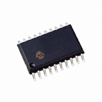
PIC16C770-I/SO Microchip Technology, PIC16C770-I/SO Datasheet - Page 117

PIC16C770-I/SO
Manufacturer Part Number
PIC16C770-I/SO
Description
IC MCU OTP 2KX14 A/D PWM 20-SOIC
Manufacturer
Microchip Technology
Series
PIC® 16Cr
Datasheets
1.PIC16C770-ISO.pdf
(220 pages)
2.PIC16C770-ISO.pdf
(6 pages)
3.PIC16C770-ISO.pdf
(8 pages)
Specifications of PIC16C770-I/SO
Core Size
8-Bit
Program Memory Size
3.5KB (2K x 14)
Peripherals
Brown-out Detect/Reset, POR, PWM, WDT
Core Processor
PIC
Speed
20MHz
Connectivity
I²C, SPI
Number Of I /o
15
Program Memory Type
OTP
Ram Size
256 x 8
Voltage - Supply (vcc/vdd)
4 V ~ 5.5 V
Data Converters
A/D 6x12b
Oscillator Type
Internal
Operating Temperature
-40°C ~ 85°C
Package / Case
20-SOIC (7.5mm Width)
Controller Family/series
PIC16C
No. Of I/o's
16
Ram Memory Size
256Byte
Cpu Speed
20MHz
No. Of Timers
3
Lead Free Status / RoHS Status
Lead free / RoHS Compliant
For Use With
ISPICR1 - ADAPTER IN-CIRCUIT PROGRAMMINGAC164028 - MODULE SKT PROMATEII 20SOIC/DIP309-1013 - ADAPTER 20-SOIC TO 20-DIP309-1012 - ADAPTER 20-SOIC TO 20-DIP
Eeprom Size
-
Lead Free Status / RoHS Status
Lead free / RoHS Compliant, Lead free / RoHS Compliant
Other names
PIC16C770I/SO
- Current page: 117 of 220
- Download datasheet (4Mb)
11.7
An A/D conversion can be started by the “special
event trigger” of the CCP module. This requires that
the CCP1M<3:0> bits be programmed as 1011b and
that the A/D module is enabled (ADON is set). When
the trigger occurs, the GO/DONE bit will be set on Q2
to start the A/D conversion and the Timer1 counter will
be reset to zero. Timer1 is RESET to automatically
repeat the A/D conversion cycle, with minimal soft-
ware overhead (moving the ADRESH and ADRESL to
the desired location). The appropriate analog input
channel must be selected before the “special event
trigger” sets the GO/DONE bit (starts a conversion
cycle).
If the A/D module is not enabled (ADON is cleared),
then the “special event trigger” will be ignored by the
A/D module, but will still RESET the Timer1 counter.
11.8
A device RESET forces all registers to their RESET
state. This forces the A/D module to be turned off, and
any conversion is aborted. The value that is in the
ADRESH and ADRESL registers are not modified.
The ADRESH and ADRESL registers will contain
unknown data after a Power-on Reset.
2002 Microchip Technology Inc.
Use of the ECCP Trigger
Effects of a RESET
11.9
Not all applications require a result with 12 bits of reso-
lution, but may instead require a faster conversion
time. The A/D module allows users to make the trade-
off of conversion speed to resolution. Regardless of
the resolution required, the acquisition time is the
same. To speed up the conversion, the A/D module
may be halted by clearing the GO/DONE bit after the
desired number of bits in the result have been con-
verted. Once the GO/DONE bit has been cleared, all
of the remaining A/D result bits are ‘0’. The equation
to determine the time before the GO/DONE bit can be
switched is as follows:
Since T
must use some method (a timer, software loop, etc.) to
determine when the A/D GO/DONE bit may be
cleared. Table 11-4 shows a comparison of time
required for a conversion with 4 bits of resolution, ver-
sus the normal 12-bit resolution conversion. The
example is for devices operating at 20 MHz. The A/D
clock is programmed for 32 T
EXAMPLE 11-4:
4-Bit Example:
12-Bit Example:
Where: N = number of bits of resolution required,
and 1T
Conversion time = (N+1)T
PIC16C717/770/771
Conversion Time = (N + 1) T
Conversion Time = (N + 1) T
AD
Faster Conversion - Lower
Resolution Trade-off
AD
is based from the device oscillator, the user
is the amplifier settling time.
4-BIT vs. 12-BIT
CONVERSION TIME
Example
= (4 + 1) T
= (5)(1.6 S)
= 8 S
= (12 + 1) T
= (13)(1.6 S)
= 20.8 S
OSC
AD
.
AD
AD
AD
DS41120B-page 115
AD
Related parts for PIC16C770-I/SO
Image
Part Number
Description
Manufacturer
Datasheet
Request
R

Part Number:
Description:
IC MCU CMOS A/D 2K 20MHZ 20-DIP
Manufacturer:
Microchip Technology
Datasheet:

Part Number:
Description:
IC MCU CMOS A/D 2K 20MHZ 20-DIP
Manufacturer:
Microchip Technology
Datasheet:

Part Number:
Description:
IC MCU OTP 2KX14 A/D PWM 20SSOP
Manufacturer:
Microchip Technology
Datasheet:

Part Number:
Description:
IC MCU OTP 2KX14 A/D PWM 20SSOP
Manufacturer:
Microchip Technology
Datasheet:

Part Number:
Description:
IC MCU EPROM2KX14 A/D PWM 20CDIP
Manufacturer:
Microchip Technology
Datasheet:

Part Number:
Description:
IC MCU OTP 2KX14 A/D PWM 20SOIC
Manufacturer:
Microchip Technology
Datasheet:

Part Number:
Description:
IC MCU CMOS A/D 2K 20MHZ 20-DIP
Manufacturer:
Microchip Technology
Datasheet:

Part Number:
Description:
IC,MICROCONTROLLER,8-BIT,PIC CPU,CMOS,SOP,20PIN,PLASTIC
Manufacturer:
Microchip Technology
Datasheet:

Part Number:
Description:
IC,MICROCONTROLLER,8-BIT,PIC CPU,CMOS,SSOP,20PIN,PLASTIC
Manufacturer:
Microchip Technology
Datasheet:

Part Number:
Description:
18/20-pin, 8-bit Cmos Microcontrollers With 10/12-bit A/d
Manufacturer:
Microchip Technology Inc.
Datasheet:

Part Number:
Description:
18/20-Pin/ 8-Bit CMOS Microcontrollers with 10/12-Bit A/D
Manufacturer:
Microchip Technology

Part Number:
Description:
18/20-Pin/ 8-Bit CMOS Microcontrollers with 10/12-Bit A/D
Manufacturer:
Microchip Technology

Part Number:
Description:
IC MCU OTP 8KX14 A/D PWM 44PLCC
Manufacturer:
Microchip Technology
Datasheet:

Part Number:
Description:
IC MCU OTP 8KX14 A/D PWM 44PLCC
Manufacturer:
Microchip Technology
Datasheet:

Part Number:
Description:
IC MCU OTP 8KX14 A/D PWM 44TQFP
Manufacturer:
Microchip Technology
Datasheet:


