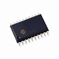
PIC16C770-I/SO Microchip Technology, PIC16C770-I/SO Datasheet - Page 7

PIC16C770-I/SO
Manufacturer Part Number
PIC16C770-I/SO
Description
IC MCU OTP 2KX14 A/D PWM 20-SOIC
Manufacturer
Microchip Technology
Series
PIC® 16Cr
Datasheets
1.PIC16C770-ISO.pdf
(220 pages)
2.PIC16C770-ISO.pdf
(6 pages)
3.PIC16C770-ISO.pdf
(8 pages)
Specifications of PIC16C770-I/SO
Core Size
8-Bit
Program Memory Size
3.5KB (2K x 14)
Peripherals
Brown-out Detect/Reset, POR, PWM, WDT
Core Processor
PIC
Speed
20MHz
Connectivity
I²C, SPI
Number Of I /o
15
Program Memory Type
OTP
Ram Size
256 x 8
Voltage - Supply (vcc/vdd)
4 V ~ 5.5 V
Data Converters
A/D 6x12b
Oscillator Type
Internal
Operating Temperature
-40°C ~ 85°C
Package / Case
20-SOIC (7.5mm Width)
Controller Family/series
PIC16C
No. Of I/o's
16
Ram Memory Size
256Byte
Cpu Speed
20MHz
No. Of Timers
3
Lead Free Status / RoHS Status
Lead free / RoHS Compliant
For Use With
ISPICR1 - ADAPTER IN-CIRCUIT PROGRAMMINGAC164028 - MODULE SKT PROMATEII 20SOIC/DIP309-1013 - ADAPTER 20-SOIC TO 20-DIP309-1012 - ADAPTER 20-SOIC TO 20-DIP
Eeprom Size
-
Lead Free Status / RoHS Status
Lead free / RoHS Compliant, Lead free / RoHS Compliant
Other names
PIC16C770I/SO
- Current page: 7 of 220
- Download datasheet (4Mb)
1.0
This document contains device-specific information.
Additional information may be found in the PICmicro
Mid-Range
(DS33023), which may be obtained from your local
Microchip Sales Representative or downloaded from
the Microchip website. The Reference Manual should
be considered a complementary document to this data
FIGURE 1-1:
OSC2/CLKOUT
2002 Microchip Technology Inc.
OSC1/CLKIN
4 MHz, 37 kHz
and ER mode
Note 1: Higher order bits are from the STATUS register.
DEVICE OVERVIEW
Internal
Program
Bus
MCU
Instruction reg
Generation
V
Instruction
Decode &
14
EPROM
DD
Program
Control
Memory
Timing
2K x 14
Enhanced CCP
, V
Family
PIC16C717 BLOCK DIAGRAM
(ECCP)
Timer0
SS
10-bit
ADC
13
Reference
Direct Addr
Program Memory
Start-up Timer
Program Counter
Brown-out
8 Level Stack
Watchdog
Read (PMR)
Power-up
Power-on
Oscillator
8
Timer
Reset
Timer
Reset
Serial Port (MSSP)
(13-bit)
Synchronous
Reference
Bandgap
Timer1
Master
Manual,
7
TM
8
3
Data Bus
Addr MUX
Registers
W reg
256 x 8
ALU
RAM
File
STATUS reg
Low-voltage
FSR reg
9
MUX
8
sheet, and is highly recommended reading for a better
understanding of the device architecture and operation
of the peripheral modules.
There are three devices (PIC16C717, PIC16C770 and
PIC16C771) covered by this data sheet. The
PIC16C717 device comes in 18/20-pin packages and
the PIC16C770/771 devices come in 20-pin packages.
The following two figures are device block diagrams of
the PIC16C717 and the PIC16C770/771.
Timer2
Detect
Addr
RAM
Indirect
PIC16C717/770/771
Addr
8
(1)
PORTA
PORTB
RA0/AN0
RA1/AN1/LVDIN
RA2/AN2/V
RA3/AN3/V
RA4/T0CKI
RA5/MCLR/V
RA6/OSC2/CLKOUT
RA7/OSC1/CLKIN
RB0/AN4/INT
RB1/AN5/SS
RB2/SCK/SCL
RB3/CCP1/P1A
RB4/SDI/SDA
RB5/SDO/P1B
RB6/T1OSO/T1CKI/P1C
RB7/T1OSI/P1D
DS41120B-page 5
REF
REF
PP
-/VRL
+/VRH
Related parts for PIC16C770-I/SO
Image
Part Number
Description
Manufacturer
Datasheet
Request
R

Part Number:
Description:
IC MCU CMOS A/D 2K 20MHZ 20-DIP
Manufacturer:
Microchip Technology
Datasheet:

Part Number:
Description:
IC MCU CMOS A/D 2K 20MHZ 20-DIP
Manufacturer:
Microchip Technology
Datasheet:

Part Number:
Description:
IC MCU OTP 2KX14 A/D PWM 20SSOP
Manufacturer:
Microchip Technology
Datasheet:

Part Number:
Description:
IC MCU OTP 2KX14 A/D PWM 20SSOP
Manufacturer:
Microchip Technology
Datasheet:

Part Number:
Description:
IC MCU EPROM2KX14 A/D PWM 20CDIP
Manufacturer:
Microchip Technology
Datasheet:

Part Number:
Description:
IC MCU OTP 2KX14 A/D PWM 20SOIC
Manufacturer:
Microchip Technology
Datasheet:

Part Number:
Description:
IC MCU CMOS A/D 2K 20MHZ 20-DIP
Manufacturer:
Microchip Technology
Datasheet:

Part Number:
Description:
IC,MICROCONTROLLER,8-BIT,PIC CPU,CMOS,SOP,20PIN,PLASTIC
Manufacturer:
Microchip Technology
Datasheet:

Part Number:
Description:
IC,MICROCONTROLLER,8-BIT,PIC CPU,CMOS,SSOP,20PIN,PLASTIC
Manufacturer:
Microchip Technology
Datasheet:

Part Number:
Description:
18/20-pin, 8-bit Cmos Microcontrollers With 10/12-bit A/d
Manufacturer:
Microchip Technology Inc.
Datasheet:

Part Number:
Description:
18/20-Pin/ 8-Bit CMOS Microcontrollers with 10/12-Bit A/D
Manufacturer:
Microchip Technology

Part Number:
Description:
18/20-Pin/ 8-Bit CMOS Microcontrollers with 10/12-Bit A/D
Manufacturer:
Microchip Technology

Part Number:
Description:
IC MCU OTP 8KX14 A/D PWM 44PLCC
Manufacturer:
Microchip Technology
Datasheet:

Part Number:
Description:
IC MCU OTP 8KX14 A/D PWM 44PLCC
Manufacturer:
Microchip Technology
Datasheet:

Part Number:
Description:
IC MCU OTP 8KX14 A/D PWM 44TQFP
Manufacturer:
Microchip Technology
Datasheet:


