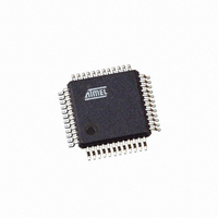
ATMEGA406-1AAU Atmel, ATMEGA406-1AAU Datasheet - Page 126

ATMEGA406-1AAU
Manufacturer Part Number
ATMEGA406-1AAU
Description
IC AVR MCU 40K 1MHZ 48LQFP
Manufacturer
Atmel
Series
AVR® ATmegar
Specifications of ATMEGA406-1AAU
Core Processor
AVR
Core Size
8-Bit
Speed
1MHz
Connectivity
I²C
Peripherals
POR, WDT
Number Of I /o
18
Program Memory Size
40KB (20K x 16)
Program Memory Type
FLASH
Eeprom Size
512 x 8
Ram Size
2K x 8
Voltage - Supply (vcc/vdd)
4 V ~ 25 V
Data Converters
A/D 10x12b
Oscillator Type
Internal
Operating Temperature
-30°C ~ 85°C
Package / Case
48-LQFP
Processor Series
ATMEGA48x
Core
AVR8
Data Bus Width
8 bit
Data Ram Size
2 KB
Interface Type
2-Wire
Maximum Clock Frequency
1 MHz
Number Of Programmable I/os
18
Number Of Timers
2
Maximum Operating Temperature
+ 85 C
Mounting Style
SMD/SMT
3rd Party Development Tools
EWAVR, EWAVR-BL
Development Tools By Supplier
ATAVRDRAGON, ATSTK500, ATSTK600, ATAVRISP2, ATAVRONEKIT
Minimum Operating Temperature
- 30 C
Cpu Family
ATmega
Device Core
AVR
Device Core Size
8b
Frequency (max)
1MHz
Total Internal Ram Size
2KB
# I/os (max)
18
Number Of Timers - General Purpose
2
Operating Supply Voltage (typ)
5/9/12/15/18/24V
Operating Supply Voltage (max)
25V
Operating Supply Voltage (min)
4V
On-chip Adc
10-chx12-bit
Instruction Set Architecture
RISC
Operating Temp Range
-30C to 85C
Operating Temperature Classification
Commercial
Mounting
Surface Mount
Pin Count
48
Package Type
LQFP
Controller Family/series
AVR MEGA
No. Of I/o's
18
Eeprom Memory Size
512Byte
Ram Memory Size
2KB
Cpu Speed
1MHz
Rohs Compliant
Yes
For Use With
770-1007 - ISP 4PORT ATMEL AVR MCU SPI/JTAG770-1005 - ISP 4PORT FOR ATMEL AVR MCU JTAG770-1004 - ISP 4PORT FOR ATMEL AVR MCU SPI
Lead Free Status / RoHS Status
Lead free / RoHS Compliant
Available stocks
Company
Part Number
Manufacturer
Quantity
Price
Part Number:
ATMEGA406-1AAU
Manufacturer:
AT
Quantity:
20 000
22.2
22.3
22.4
126
Deep Under-voltage Protection
Discharge Over-current Protection
Charge Over-current Protection
ATmega406
The Deep Under-voltage Protection ensures that the battery cells will not be discharged deeper
than the programmable Deep Under-voltage detection level. If the voltage at the VFET pin is
below this level for a time longer than the programmable delay time, C-FET, PC-FET and D-FET
are automatically switched off and the chip enters Power-off mode. The Deep Under-voltage
Early Warning interrupt flag (DUVIF) will be set 250 ms before the chip enters Power-off. This
will give the CPU a chance to take necessary actions before the power is switched off.
The device will remain in the Power-off mode until a charger is connected. When a charger is
detected, a normal power-up sequence is started and the chip initializes to default state.
The Deep Under-voltage delay time and Deep Under-voltage detection level are set in the Bat-
tery Protection Deep Under-voltage Register (BPDUV). The Parameter Registers can be locked
after the initial configuration, prohibiting any further updates until the next Hardware Reset.
Refer to
The Current Battery Protection (CBP) monitors the cell current by sampling the shunt resistor
voltage at the PPI/NNI input pins. A differential operational amplifier amplifies the voltage with a
suitable gain. The output from the operational amplifier is compared to an accurate, programma-
ble On-chip voltage reference by an Analog Comparator. If the shunt resistor voltage is above
the Discharge Over-current Detection level for a time longer than Over-current Protection Reac-
tion Time, the chip activates Discharge Over-current Protection. A sampled system clocked by
the internal ULP Oscillator is used for Over-current and Short-circuit Protection. This ensures a
reliable clock source, off-set cancellation and low power consumption.
When the Discharge Over-current Protection is activated, the external D-FET, PC-FET, and C-
FET are disabled and a Current Protection Timer is started. This timer ensures that the FETs are
disabled for at least one second. The application software must then set the DFE and CFE bits
in the FET Control and Status Register to re-enable normal operation. If the D-FET is re-enabled
while the loading of the battery still is too large, the Discharge Over-current Protection will be
activated again.
If the voltage at the PPI/NNI pins is above the Charge Over-current Detection level for a time
longer than Over-current Protection Reaction Time, the chip activates Charge Over-current
Protection.
When the Charge Over-current Protection is activated, the external D-FET, PC-FET, and C-FET
are disabled and a Current Protection Timer is started. This timer ensures that the FETs are dis-
abled for at least one second. The application software must then set the DFE and CFE bits in
the FET Control and Status Register to re-enable normal operation. If the C-FET is re-enabled
and the charger continues to supply too high currents, the Charge Over-current Protection will
be activated again.
”Register Description for Battery Protection” on page 128
for register descriptions.
2548E–AVR–07/06


