ATMEGA406-1AAU Atmel, ATMEGA406-1AAU Datasheet - Page 174
ATMEGA406-1AAU
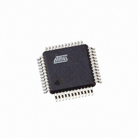
Manufacturer Part Number
ATMEGA406-1AAU
Description
IC AVR MCU 40K 1MHZ 48LQFP
Manufacturer
Atmel
Series
AVR® ATmegar
Specifications of ATMEGA406-1AAU
Core Processor
AVR
Core Size
8-Bit
Speed
1MHz
Connectivity
I²C
Peripherals
POR, WDT
Number Of I /o
18
Program Memory Size
40KB (20K x 16)
Program Memory Type
FLASH
Eeprom Size
512 x 8
Ram Size
2K x 8
Voltage - Supply (vcc/vdd)
4 V ~ 25 V
Data Converters
A/D 10x12b
Oscillator Type
Internal
Operating Temperature
-30°C ~ 85°C
Package / Case
48-LQFP
Processor Series
ATMEGA48x
Core
AVR8
Data Bus Width
8 bit
Data Ram Size
2 KB
Interface Type
2-Wire
Maximum Clock Frequency
1 MHz
Number Of Programmable I/os
18
Number Of Timers
2
Maximum Operating Temperature
+ 85 C
Mounting Style
SMD/SMT
3rd Party Development Tools
EWAVR, EWAVR-BL
Development Tools By Supplier
ATAVRDRAGON, ATSTK500, ATSTK600, ATAVRISP2, ATAVRONEKIT
Minimum Operating Temperature
- 30 C
Cpu Family
ATmega
Device Core
AVR
Device Core Size
8b
Frequency (max)
1MHz
Total Internal Ram Size
2KB
# I/os (max)
18
Number Of Timers - General Purpose
2
Operating Supply Voltage (typ)
5/9/12/15/18/24V
Operating Supply Voltage (max)
25V
Operating Supply Voltage (min)
4V
On-chip Adc
10-chx12-bit
Instruction Set Architecture
RISC
Operating Temp Range
-30C to 85C
Operating Temperature Classification
Commercial
Mounting
Surface Mount
Pin Count
48
Package Type
LQFP
Controller Family/series
AVR MEGA
No. Of I/o's
18
Eeprom Memory Size
512Byte
Ram Memory Size
2KB
Cpu Speed
1MHz
Rohs Compliant
Yes
For Use With
770-1007 - ISP 4PORT ATMEL AVR MCU SPI/JTAG770-1005 - ISP 4PORT FOR ATMEL AVR MCU JTAG770-1004 - ISP 4PORT FOR ATMEL AVR MCU SPI
Lead Free Status / RoHS Status
Lead free / RoHS Compliant
Available stocks
Company
Part Number
Manufacturer
Quantity
Price

Part Number:
ATMEGA406-1AAU
Manufacturer:
AT
Quantity:
20 000


26.5
174
Using the On-chip Debug System
ATmega406
• Apply the TMS sequence 1, 1, 0 to re-enter the Run-Test/Idle state. The instruction is latched
• At the TMS input, apply the sequence 1, 0, 0 at the rising edges of TCK to enter the Shift Data
• Apply the TMS sequence 1, 1, 0 to re-enter the Run-Test/Idle state. If the selected data register
As shown in the state diagram, the Run-Test/Idle state need not be entered between selecting
JTAG instruction and using data registers, and some JTAG instructions may select certain func-
tions to be performed in the Run-Test/Idle, making it unsuitable as an Idle state.
Note:
For detailed information on the JTAG specification, refer to the literature listed in
face and On-chip Debug System” on page
As shown in
• A scan chain on the interface between the internal AVR CPU and the internal peripheral units.
• Break Point unit.
• Communication interface between the CPU and JTAG system.
All read or modify/write operations needed for implementing the Debugger are done by applying
AVR instructions via the internal AVR CPU Scan Chain. The CPU sends the result to an I/O
memory mapped location which is part of the communication interface between the CPU and the
JTAG system.
The Break Point Unit implements Break on Change of Program Flow, Single Step Break, two
Program Memory Break Points, and two combined Break Points. Together, the four Break
Points can be configured as either:
• 4 single Program Memory Break Points.
• 3 Single Program Memory Break Point + 1 single Data Memory Break Point.
• 2 single Program Memory Break Points + 2 single Data Memory Break Points.
• 2 single Program Memory Break Points + 1 Program Memory Break Point with mask (“range
• 2 single Program Memory Break Points + 1 Data Memory Break Point with mask (“range Break
A debugger, like the AVR Studio, may however use one or more of these resources for its inter-
nal purpose, leaving less flexibility to the end-user.
A list of the On-chip Debug specific JTAG instructions is given in
Instructions” on page
onto the parallel output from the Shift Register path in the Update-IR state. The Exit-IR, Pause-
IR, and Exit2-IR states are only used for navigating the state machine.
Register – Shift-DR state. While in this state, upload the selected data register (selected by the
present JTAG instruction in the JTAG Instruction Register) from the TDI input at the rising edge
of TCK. In order to remain in the Shift-DR state, the TMS input must be held low during input of
all bits except the MSB. The MSB of the data is shifted in when this state is left by setting TMS
high. While the data register is shifted in from the TDI pin, the parallel inputs to the data
register captured in the Capture-DR state is shifted out on the TDO pin.
has a latched parallel-output, the latching takes place in the Update-DR state. The Exit-DR,
Pause-DR, and Exit2-DR states are only used for navigating the state machine.
Break Point”).
Point”).
Independent of the initial state of the TAP Controller, the Test-Logic-Reset state can always be
entered by holding TMS high for five TCK clock periods.
Figure
26-1, the hardware support for On-chip Debugging consists mainly of
175.
171.
”On-chip Debug Specific JTAG
2548E–AVR–07/06
”JTAG Inter-
Related parts for ATMEGA406-1AAU
Image
Part Number
Description
Manufacturer
Datasheet
Request
R

Part Number:
Description:
Manufacturer:
Atmel Corporation
Datasheet:

Part Number:
Description:
IC AVR MCU 2.4GHZ XCEIVER 64QFN
Manufacturer:
Atmel
Datasheet:

Part Number:
Description:
Manufacturer:
Atmel
Datasheet:

Part Number:
Description:
MCU ATMEGA644/AT86RF230 40-DIP
Manufacturer:
Atmel
Datasheet:
Part Number:
Description:
BUNDLE ATMEGA644P/AT86RF230 QFN
Manufacturer:
Atmel
Datasheet:

Part Number:
Description:
BUNDLE ATMEGA644P/AT86RF230 TQFP
Manufacturer:
Atmel
Datasheet:

Part Number:
Description:
MCU ATMEGA1281/AT86RF230 64-TQFP
Manufacturer:
Atmel
Datasheet:

Part Number:
Description:
MCU ATMEGA1280/AT86RF230 100TQFP
Manufacturer:
Atmel
Datasheet:
Part Number:
Description:
BUNDLE ATMEGA1280/AT86RF100-TQFP
Manufacturer:
Atmel
Datasheet:

Part Number:
Description:
BUNDLE ATMEGA2560V/AT86RF230-ZU
Manufacturer:
Atmel
Datasheet:
Part Number:
Description:
MCU ATMEGA2561/AT86RF230 64-TQFP
Manufacturer:
Atmel
Datasheet:
Part Number:
Description:
MCU ATMEGA2560/AT86RF230 100TQFP
Manufacturer:
Atmel
Datasheet:
Part Number:
Description:
MCU ATMEGA2561/AT86RF230 64-QFN
Manufacturer:
Atmel
Datasheet:

Part Number:
Description:
MCU, 8BIT, AVR, 16K FLASH, 28PDIP
Manufacturer:
Atmel
Datasheet:

Part Number:
Description:
Microcontroller Modules MCU CARD BIGAVR6 100P W/ ATMEGA2560
Manufacturer:
mikroElektronika