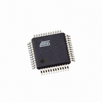
ATMEGA406-1AAU Atmel, ATMEGA406-1AAU Datasheet - Page 147

ATMEGA406-1AAU
Manufacturer Part Number
ATMEGA406-1AAU
Description
IC AVR MCU 40K 1MHZ 48LQFP
Manufacturer
Atmel
Series
AVR® ATmegar
Specifications of ATMEGA406-1AAU
Core Processor
AVR
Core Size
8-Bit
Speed
1MHz
Connectivity
I²C
Peripherals
POR, WDT
Number Of I /o
18
Program Memory Size
40KB (20K x 16)
Program Memory Type
FLASH
Eeprom Size
512 x 8
Ram Size
2K x 8
Voltage - Supply (vcc/vdd)
4 V ~ 25 V
Data Converters
A/D 10x12b
Oscillator Type
Internal
Operating Temperature
-30°C ~ 85°C
Package / Case
48-LQFP
Processor Series
ATMEGA48x
Core
AVR8
Data Bus Width
8 bit
Data Ram Size
2 KB
Interface Type
2-Wire
Maximum Clock Frequency
1 MHz
Number Of Programmable I/os
18
Number Of Timers
2
Maximum Operating Temperature
+ 85 C
Mounting Style
SMD/SMT
3rd Party Development Tools
EWAVR, EWAVR-BL
Development Tools By Supplier
ATAVRDRAGON, ATSTK500, ATSTK600, ATAVRISP2, ATAVRONEKIT
Minimum Operating Temperature
- 30 C
Cpu Family
ATmega
Device Core
AVR
Device Core Size
8b
Frequency (max)
1MHz
Total Internal Ram Size
2KB
# I/os (max)
18
Number Of Timers - General Purpose
2
Operating Supply Voltage (typ)
5/9/12/15/18/24V
Operating Supply Voltage (max)
25V
Operating Supply Voltage (min)
4V
On-chip Adc
10-chx12-bit
Instruction Set Architecture
RISC
Operating Temp Range
-30C to 85C
Operating Temperature Classification
Commercial
Mounting
Surface Mount
Pin Count
48
Package Type
LQFP
Controller Family/series
AVR MEGA
No. Of I/o's
18
Eeprom Memory Size
512Byte
Ram Memory Size
2KB
Cpu Speed
1MHz
Rohs Compliant
Yes
For Use With
770-1007 - ISP 4PORT ATMEL AVR MCU SPI/JTAG770-1005 - ISP 4PORT FOR ATMEL AVR MCU JTAG770-1004 - ISP 4PORT FOR ATMEL AVR MCU SPI
Lead Free Status / RoHS Status
Lead free / RoHS Compliant
Available stocks
Company
Part Number
Manufacturer
Quantity
Price
Part Number:
ATMEGA406-1AAU
Manufacturer:
AT
Quantity:
20 000
25.6
25.6.1
25.6.2
2548E–AVR–07/06
TWI Register Description
TWBR – TWI Bit Rate Register
TWCR – TWI Control Register
• Bits 7:0 – TWI Bit Rate Register
TWBR selects the division factor for the bit rate generator. The bit rate generator is a frequency
divider which generates the SCL clock frequency in the Master modes. See
Unit” on page 145
The TWCR is used to control the operation of the TWI. It is used to enable the TWI, to initiate a
Master access by applying a START condition to the bus, to generate a Receiver acknowledge,
to generate a stop condition, and to control halting of the bus while the data to be written to the
bus are written to the TWDR. It also indicates a write collision if data is attempted written to
TWDR while the register is inaccessible.
• Bit 7 – TWINT: TWI Interrupt Flag
This bit is set by hardware when the TWI has finished its current job and expects application
software response. If the I-bit in SREG and TWIE in TWCR are set, the MCU will jump to the
TWI Interrupt Vector. While the TWINT flag is set, the SCL low period is stretched. The TWINT
flag must be cleared by software by writing a logic one to it. Note that this flag is not automati-
cally cleared by hardware when executing the interrupt routine. Also note that clearing this flag
starts the operation of the TWI, so all accesses to the TWI Address Register (TWAR), TWI Sta-
tus Register (TWSR), and TWI Data Register (TWDR) must be complete before clearing this
flag.
• Bit 6 – TWEA: TWI Enable Acknowledge Bit
The TWEA bit controls the generation of the acknowledge pulse. If the TWEA bit is written to
one, the ACK pulse is generated on the TWI bus if the following conditions are met:
1. The device’s own slave address has been received.
2. A general call has been received, while the TWGCE bit in the TWAR is set.
3. A data byte has been received in Master Receiver or Slave Receiver mode.
By writing the TWEA bit to zero, the device can be virtually disconnected from the Two-wire
Serial Bus temporarily. Address recognition can then be resumed by writing the TWEA bit to one
again.
• Bit 5 – TWSTA: TWI START Condition Bit
The application writes the TWSTA bit to one when it desires to become a Master on the Two-
wire Serial Bus. The TWI hardware checks if the bus is available, and generates a START con-
Bit
(0xB8)
Read/Write
Initial Value
Bit
(0xBC)
Read/Write
Initial Value
TWBR7
TWINT
R/W
R/W
7
0
7
0
for calculating bit rates.
TWBR6
TWEA
R/W
R/W
6
0
6
0
TWBR5
TWSTA
R/W
R/W
5
0
5
0
TWSTO
TWBR4
R/W
R/W
4
0
4
0
TWBR3
TWWC
R/W
R
3
0
3
0
TWBR2
TWEN
R/W
R/W
2
0
2
0
TWBR1
R/W
R
1
0
1
–
0
ATmega406
”Bit Rate Generator
TWBR0
TWIE
R/W
R/W
0
0
0
0
TWBR
TWCR
147


