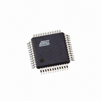
ATMEGA406-1AAU Atmel, ATMEGA406-1AAU Datasheet - Page 133

ATMEGA406-1AAU
Manufacturer Part Number
ATMEGA406-1AAU
Description
IC AVR MCU 40K 1MHZ 48LQFP
Manufacturer
Atmel
Series
AVR® ATmegar
Specifications of ATMEGA406-1AAU
Core Processor
AVR
Core Size
8-Bit
Speed
1MHz
Connectivity
I²C
Peripherals
POR, WDT
Number Of I /o
18
Program Memory Size
40KB (20K x 16)
Program Memory Type
FLASH
Eeprom Size
512 x 8
Ram Size
2K x 8
Voltage - Supply (vcc/vdd)
4 V ~ 25 V
Data Converters
A/D 10x12b
Oscillator Type
Internal
Operating Temperature
-30°C ~ 85°C
Package / Case
48-LQFP
Processor Series
ATMEGA48x
Core
AVR8
Data Bus Width
8 bit
Data Ram Size
2 KB
Interface Type
2-Wire
Maximum Clock Frequency
1 MHz
Number Of Programmable I/os
18
Number Of Timers
2
Maximum Operating Temperature
+ 85 C
Mounting Style
SMD/SMT
3rd Party Development Tools
EWAVR, EWAVR-BL
Development Tools By Supplier
ATAVRDRAGON, ATSTK500, ATSTK600, ATAVRISP2, ATAVRONEKIT
Minimum Operating Temperature
- 30 C
Cpu Family
ATmega
Device Core
AVR
Device Core Size
8b
Frequency (max)
1MHz
Total Internal Ram Size
2KB
# I/os (max)
18
Number Of Timers - General Purpose
2
Operating Supply Voltage (typ)
5/9/12/15/18/24V
Operating Supply Voltage (max)
25V
Operating Supply Voltage (min)
4V
On-chip Adc
10-chx12-bit
Instruction Set Architecture
RISC
Operating Temp Range
-30C to 85C
Operating Temperature Classification
Commercial
Mounting
Surface Mount
Pin Count
48
Package Type
LQFP
Controller Family/series
AVR MEGA
No. Of I/o's
18
Eeprom Memory Size
512Byte
Ram Memory Size
2KB
Cpu Speed
1MHz
Rohs Compliant
Yes
For Use With
770-1007 - ISP 4PORT ATMEL AVR MCU SPI/JTAG770-1005 - ISP 4PORT FOR ATMEL AVR MCU JTAG770-1004 - ISP 4PORT FOR ATMEL AVR MCU SPI
Lead Free Status / RoHS Status
Lead free / RoHS Compliant
Available stocks
Company
Part Number
Manufacturer
Quantity
Price
Part Number:
ATMEGA406-1AAU
Manufacturer:
AT
Quantity:
20 000
23. FET Control
2548E–AVR–07/06
In addition to the FET disable control signals from the battery protection circuitry, the CPU may
disable the Charge FET (C-FET), the Discharge FET (D-FET), or both, by writing to the FET
Control Register. Note that the CPU is never allowed to enable a FET that is disabled by the bat-
tery protection circuitry. The FET control is shown in
The PWM output from the 8-bit Timer/Counter0, OC0B, can be configured to drive the C-FET,
Precharge FET (PC-FET) or both directly. This can be useful for controlling the charging of the
battery cells. The PWM is configured by the COM0B1:0 and WGM02:0 bits in the
TCCR0A/TCCR0B registers. Note that the OC0B pins does not need to be configured as an out-
put. This means that the PWM output can be used to drive the C-FET and/or the PC-FET
without occupying the OC0B-pin.
If C-FET is disabled and D-FET enabled, discharge current will run through the body-drain diode
of the C-FET and vice versa. To avoid the potential heat problem from this situation, software
must ensure that D-FET is not disabled when a charge current is flowing, and that C-FET is not
disabled when a discharge current is flowing.
If the battery has been deeply discharged, large surge currents may result when a charger is
connected. In this case, it is recommended to first pre charge the battery through a current limit-
ing resistor. For this purpose, ATmega406 provides a Precharge FET (PC-FET) control output.
This output is default enabled.
If ATmega406 has entered the Power-off mode, all FET control outputs will be disabled. When a
charger is connected, the CPU will wake up. When waking up from Power-off mode, the C-FET
and D-FET control outputs will remain disabled while PC-FET is default enabled. When the CPU
detects that the cell voltages have risen enough to allow normal charging, it should enable the
C-FET and D-FET control outputs and disable the PC-FET control output.
If the Current Battery Protection has been activated, the Current Protection Timer will ensure a
hold-off time of 1 second before software can re-enable the external FETs.
Figure 23-1. FET Control Block Diagram
Power-off Mode
CURRENT_PROTECTION
OC0B
Register
Control
Status
FET
and
Current Protection
PWMOC
CFE
PWMOPC
PFD
DFE
Timer
Figure 23-1 on page
1
0
1
0
ATmega406
133.
Driver
Driver
Driver
FET
FET
FET
OC
OPC
OD
133


