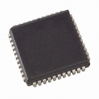
AT89C51RE2-SLSUM Atmel, AT89C51RE2-SLSUM Datasheet - Page 135

AT89C51RE2-SLSUM
Manufacturer Part Number
AT89C51RE2-SLSUM
Description
MCU 8BIT FLASH 2.7-5.5V 44-PLCC
Manufacturer
Atmel
Series
89Cr
Datasheet
1.AT89C51RE2-SLSUM.pdf
(187 pages)
Specifications of AT89C51RE2-SLSUM
Core Processor
8051
Core Size
8-Bit
Speed
60MHz
Connectivity
I²C, SPI, UART/USART
Peripherals
POR, PWM, WDT
Number Of I /o
34
Program Memory Size
128KB (128K x 8)
Program Memory Type
FLASH
Ram Size
8K x 8
Voltage - Supply (vcc/vdd)
2.7 V ~ 5.5 V
Oscillator Type
External
Operating Temperature
-40°C ~ 85°C
Package / Case
44-PLCC
Package
44PLCC
Device Core
8051
Family Name
89C
Maximum Speed
40 MHz
Operating Supply Voltage
3.3|5 V
Data Bus Width
8 Bit
Number Of Programmable I/os
34
Interface Type
SPI/TWI/UART
Number Of Timers
3
Processor Series
AT89x
Core
8051
Data Ram Size
8 KB
Maximum Clock Frequency
40 MHz
Maximum Operating Temperature
+ 85 C
Mounting Style
SMD/SMT
3rd Party Development Tools
PK51, CA51, A51, ULINK2
Development Tools By Supplier
AT89OCD-01
Minimum Operating Temperature
- 40 C
Cpu Family
89C
Device Core Size
8b
Frequency (max)
40MHz
Total Internal Ram Size
8KB
# I/os (max)
34
Number Of Timers - General Purpose
3
Operating Supply Voltage (typ)
3.3/5V
Operating Supply Voltage (max)
5.5V
Operating Supply Voltage (min)
2.7V
Instruction Set Architecture
CISC
Operating Temp Range
-40C to 85C
Operating Temperature Classification
Industrial
Mounting
Surface Mount
Pin Count
44
Package Type
PLCC
For Use With
AT89OCD-01 - USB EMULATOR FOR AT8XC51 MCUAT89STK-11 - KIT STARTER FOR AT89C51RX2
Lead Free Status / RoHS Status
Lead free / RoHS Compliant
Eeprom Size
-
Data Converters
-
Lead Free Status / Rohs Status
Lead free / RoHS Compliant
Available stocks
Company
Part Number
Manufacturer
Quantity
Price
Company:
Part Number:
AT89C51RE2-SLSUM
Manufacturer:
HONEYWELL
Quantity:
101
Slave Receiver Mode
Slave Transmitter Mode
7663D–8051–10/08
When the slave address and the direction bit have been transmitted and an acknowl-
edgement bit has been received, the serial interrupt flag is set again and a number of
status code in SSCS are possible. There are 40h, 48h or 38h for the master mode and
also 68h, 78h or B0h if the slave mode was enabled (AA=logic 1). The appropriate
action to be taken for each of these status code is detailed in Table . This scheme is
repeated until a STOP condition is transmitted.
SSIE, CR2, CR1 and CR0 are not affected by the serial transfer and are referred to
Table 7 to Table 11. After a repeated START condition (state 10h) the TWI module may
switch to the master transmitter mode by loading SSDAT with SLA+W.
In the slave receiver mode, a number of data bytes are received from a master transmit-
ter (Figure 54). To initiate the slave receiver mode, SSADR and SSCON must be loaded
as follows:
Table 99. SSADR: Slave Receiver Mode Initialization
The upper 7 bits are the address to which the TWI module will respond when addressed
by a master. If the LSB (GC) is set the TWI module will respond to the general call
address (00h); otherwise it ignores the general call address.
Table 100. SSCON: Slave Receiver Mode Initialization
CR0, CR1 and CR2 have no effect in the slave mode. SSIE must be set to enable the
TWI. The AA bit must be set to enable the own slave address or the general call address
acknowledgement. STA, STO and SI must be cleared.
When SSADR and SSCON have been initialised, the TWI module waits until it is
addressed by its own slave address followed by the data direction bit which must be at
logic 0 (W) for the TWI to operate in the slave receiver mode. After its own slave
address and the W bit have been received, the serial interrupt flag is set and a valid sta-
tus code can be read from SSCS. This status code is used to vector to an interrupt
service routine.The appropriate action to be taken for each of these status code is
detailed in Table . The slave receiver mode may also be entered if arbitration is lost
while TWI is in the master mode (states 68h and 78h).
If the AA bit is reset during a transfer, TWI module will return a not acknowledge (logic 1)
to SDA after the next received data byte. While AA is reset, the TWI module does not
respond to its own slave address. However, the 2-wire bus is still monitored and
address recognition may be resume at any time by setting AA. This means that the AA
bit may be used to temporarily isolate the module from the 2-wire bus.
In the slave transmitter mode, a number of data bytes are transmitted to a master
receiver (Figure 55). Data transfer is initialized as in the slave receiver mode. When
SSADR and SSCON have been initialized, the TWI module waits until it is addressed by
bit rate
CR2
A6
SSIE
A5
1
STA
A4
0
own slave address
STO
A3
0
A2
SI
0
AA
A1
1
AT89C51RE2
bit rate
CR1
A0
bit rate
CR0
GC
135


