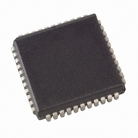
AT89C51RE2-SLSUM Atmel, AT89C51RE2-SLSUM Datasheet - Page 71

AT89C51RE2-SLSUM
Manufacturer Part Number
AT89C51RE2-SLSUM
Description
MCU 8BIT FLASH 2.7-5.5V 44-PLCC
Manufacturer
Atmel
Series
89Cr
Datasheet
1.AT89C51RE2-SLSUM.pdf
(187 pages)
Specifications of AT89C51RE2-SLSUM
Core Processor
8051
Core Size
8-Bit
Speed
60MHz
Connectivity
I²C, SPI, UART/USART
Peripherals
POR, PWM, WDT
Number Of I /o
34
Program Memory Size
128KB (128K x 8)
Program Memory Type
FLASH
Ram Size
8K x 8
Voltage - Supply (vcc/vdd)
2.7 V ~ 5.5 V
Oscillator Type
External
Operating Temperature
-40°C ~ 85°C
Package / Case
44-PLCC
Package
44PLCC
Device Core
8051
Family Name
89C
Maximum Speed
40 MHz
Operating Supply Voltage
3.3|5 V
Data Bus Width
8 Bit
Number Of Programmable I/os
34
Interface Type
SPI/TWI/UART
Number Of Timers
3
Processor Series
AT89x
Core
8051
Data Ram Size
8 KB
Maximum Clock Frequency
40 MHz
Maximum Operating Temperature
+ 85 C
Mounting Style
SMD/SMT
3rd Party Development Tools
PK51, CA51, A51, ULINK2
Development Tools By Supplier
AT89OCD-01
Minimum Operating Temperature
- 40 C
Cpu Family
89C
Device Core Size
8b
Frequency (max)
40MHz
Total Internal Ram Size
8KB
# I/os (max)
34
Number Of Timers - General Purpose
3
Operating Supply Voltage (typ)
3.3/5V
Operating Supply Voltage (max)
5.5V
Operating Supply Voltage (min)
2.7V
Instruction Set Architecture
CISC
Operating Temp Range
-40C to 85C
Operating Temperature Classification
Industrial
Mounting
Surface Mount
Pin Count
44
Package Type
PLCC
For Use With
AT89OCD-01 - USB EMULATOR FOR AT8XC51 MCUAT89STK-11 - KIT STARTER FOR AT89C51RX2
Lead Free Status / RoHS Status
Lead free / RoHS Compliant
Eeprom Size
-
Data Converters
-
Lead Free Status / Rohs Status
Lead free / RoHS Compliant
Available stocks
Company
Part Number
Manufacturer
Quantity
Price
Company:
Part Number:
AT89C51RE2-SLSUM
Manufacturer:
HONEYWELL
Quantity:
101
Timer 1
Mode 0 (13-bit Timer)
Mode 1 (16-bit Timer)
Mode 2 (8-bit Timer
with Auto-Reload)
Mode 3 (Halt)
Interrupt
7663E–8051–10/08
Timer 1 is identical to Timer 0 excepted for Mode 3 which is a hold-count mode. The following
comments help to understand the differences:
•
•
•
•
•
•
•
Mode 0 configures Timer 1 as a 13-bit Timer, which is set up as an 8-bit Timer (TH1 register)
with a modulo-32 prescaler implemented with the lower 5 bits of the TL1 register (see
Figure 23). The upper 3 bits of TL1 register are ignored. Prescaler overflow increments TH1
register.
Mode 1 configures Timer 1 as a 16-bit Timer with TH1 and TL1 registers connected in cascade
(see Figure 24). The selected input increments TL1 register.
Mode 2 configures Timer 1 as an 8-bit Timer (TL1 register) with automatic reload from TH1 reg-
ister on overflow (see Figure 25). TL1 overflow sets TF1 flag in TCON register and reloads TL1
with the contents of TH1, which is preset by software. The reload leaves TH1 unchanged.
Placing Timer 1 in mode 3 causes it to halt and hold its count. This can be used to halt Timer 1
when TR1 run control bit is not available i.e. when Timer 0 is in mode 3.
Each Timer handles one interrupt source that is the timer overflow flag TF0 or TF1. This flag is
set every time an overflow occurs. Flags are cleared when vectoring to the Timer interrupt rou-
tine. Interrupts are enabled by setting
globally enabled by setting EA bit in IEN0 register.
Timer 1 functions as either a Timer or event Counter in three modes of operation. Figure 23
to Figure 25 show the logical configuration for modes 0, 1, and 2. Timer 1’s mode 3 is a
hold-count mode.
Timer 1 is controlled by the four high-order bits of TMOD register (see Figure 47) and bits 2,
3, 6 and 7 of TCON register (see Figure 46). TMOD register selects the method of Timer
gating (GATE1), Timer or Counter operation (C/T1#) and mode of operation (M11 and M01).
TCON register provides Timer 1 control functions: overflow flag (TF1), run control bit (TR1),
interrupt flag (IE1) and interrupt type control bit (IT1).
Timer 1 can serve as the Baud Rate Generator for the Serial Port. Mode 2 is best suited for
this purpose.
For normal Timer operation (GATE1 = 0), setting TR1 allows TL1 to be incremented by the
selected input. Setting GATE1 and TR1 allows external pin INT1# to control Timer operation.
Timer 1 overflow (count rolls over from all 1s to all 0s) sets the TF1 flag generating an
interrupt request.
When Timer 0 is in mode 3, it uses Timer 1’s overflow flag (TF1) and run control bit (TR1).
For this situation, use Timer 1 only for applications that do not require an interrupt (such as a
Baud Rate Generator for the Serial Port) and switch Timer 1 in and out of mode 3 to turn it
off and on.
It is important to stop Timer/Counter before changing mode.
ETx
bit in IEN0 register. This assumes interrupts are
AT89C51RE2
71


