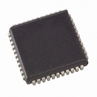
AT89C51RE2-SLSUM Atmel, AT89C51RE2-SLSUM Datasheet - Page 19

AT89C51RE2-SLSUM
Manufacturer Part Number
AT89C51RE2-SLSUM
Description
MCU 8BIT FLASH 2.7-5.5V 44-PLCC
Manufacturer
Atmel
Series
89Cr
Datasheet
1.AT89C51RE2-SLSUM.pdf
(187 pages)
Specifications of AT89C51RE2-SLSUM
Core Processor
8051
Core Size
8-Bit
Speed
60MHz
Connectivity
I²C, SPI, UART/USART
Peripherals
POR, PWM, WDT
Number Of I /o
34
Program Memory Size
128KB (128K x 8)
Program Memory Type
FLASH
Ram Size
8K x 8
Voltage - Supply (vcc/vdd)
2.7 V ~ 5.5 V
Oscillator Type
External
Operating Temperature
-40°C ~ 85°C
Package / Case
44-PLCC
Package
44PLCC
Device Core
8051
Family Name
89C
Maximum Speed
40 MHz
Operating Supply Voltage
3.3|5 V
Data Bus Width
8 Bit
Number Of Programmable I/os
34
Interface Type
SPI/TWI/UART
Number Of Timers
3
Processor Series
AT89x
Core
8051
Data Ram Size
8 KB
Maximum Clock Frequency
40 MHz
Maximum Operating Temperature
+ 85 C
Mounting Style
SMD/SMT
3rd Party Development Tools
PK51, CA51, A51, ULINK2
Development Tools By Supplier
AT89OCD-01
Minimum Operating Temperature
- 40 C
Cpu Family
89C
Device Core Size
8b
Frequency (max)
40MHz
Total Internal Ram Size
8KB
# I/os (max)
34
Number Of Timers - General Purpose
3
Operating Supply Voltage (typ)
3.3/5V
Operating Supply Voltage (max)
5.5V
Operating Supply Voltage (min)
2.7V
Instruction Set Architecture
CISC
Operating Temp Range
-40C to 85C
Operating Temperature Classification
Industrial
Mounting
Surface Mount
Pin Count
44
Package Type
PLCC
For Use With
AT89OCD-01 - USB EMULATOR FOR AT8XC51 MCUAT89STK-11 - KIT STARTER FOR AT89C51RX2
Lead Free Status / RoHS Status
Lead free / RoHS Compliant
Eeprom Size
-
Data Converters
-
Lead Free Status / Rohs Status
Lead free / RoHS Compliant
Available stocks
Company
Part Number
Manufacturer
Quantity
Price
Company:
Part Number:
AT89C51RE2-SLSUM
Manufacturer:
HONEYWELL
Quantity:
101
7663E–8051–10/08
Table 17. AUXR1 register
AUXR1- Auxiliary Register 1(0A2h)
Reset Value: XX0X XX0X0b
Not bit addressable
Note:
ASSEMBLY LANGUAGE
Number
; Block move using dual data pointers
; Modifies DPTR0, DPTR1, A and PSW
; note: DPS exits opposite of entry state
; unless an extra INC AUXR1 is added
;
00A2
;
0000 909000MOV DPTR,#SOURCE ; address of SOURCE
0003 05A2 INC AUXR1 ; switch data pointers
0005 90A000 MOV DPTR,#DEST ; address of DEST
0008
0008 05A2 INC AUXR1 ; switch data pointers
000A E0 MOVX A,@DPTR ; get a byte from SOURCE
000B A3 INC DPTR ; increment SOURCE address
000C 05A2 INC AUXR1 ; switch data pointers
000E F0 MOVX @DPTR,A ; write the byte to DEST
000F A3 INC DPTR ; increment DEST address
EES
Bit
7
7
6
5
4
3
2
1
0
*Bit 2 stuck at 0; this allows to use INC AUXR1 to toggle DPS without changing GF3.
LOOP:
AUXR1 EQU 0A2H
Mnemonic
DPS
SP9
EES
SP9
GF2
Bit
U2
6
0
-
-
Description
Enable Extended Stack
Set to enable the extended stack
Clear to disable the extended stack (default value)
Stack Pointer 9th Bit
This bit has no effect when the EES bit is cleared.
Set when the stack pointer belongs to the XRAM memory space
Cleared when the stack pointer belongs to the 256bytes of internal RAM.
P4 bit addressable
Clear to map SCON_1 register at C0h sfr address
Set to map P4 port register at C0h address.
Reserved
Reserved
Data Pointer Selection
U2
5
This bit allows the selection of the stack extended mode.
The value read from this bit is indeterminate. Do not set this bit.
This bit is a general purpose user flag. *
Always cleared.
The value read from this bit is indeterminate. Do not set this bit.
Cleared to select DPTR0.
Set to select DPTR1.
4
-
GF2
3
2
0
AT89C51RE2
1
-
DPS
0
19


