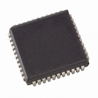
AT89C51RE2-SLSUM Atmel, AT89C51RE2-SLSUM Datasheet - Page 6

AT89C51RE2-SLSUM
Manufacturer Part Number
AT89C51RE2-SLSUM
Description
MCU 8BIT FLASH 2.7-5.5V 44-PLCC
Manufacturer
Atmel
Series
89Cr
Datasheet
1.AT89C51RE2-SLSUM.pdf
(187 pages)
Specifications of AT89C51RE2-SLSUM
Core Processor
8051
Core Size
8-Bit
Speed
60MHz
Connectivity
I²C, SPI, UART/USART
Peripherals
POR, PWM, WDT
Number Of I /o
34
Program Memory Size
128KB (128K x 8)
Program Memory Type
FLASH
Ram Size
8K x 8
Voltage - Supply (vcc/vdd)
2.7 V ~ 5.5 V
Oscillator Type
External
Operating Temperature
-40°C ~ 85°C
Package / Case
44-PLCC
Package
44PLCC
Device Core
8051
Family Name
89C
Maximum Speed
40 MHz
Operating Supply Voltage
3.3|5 V
Data Bus Width
8 Bit
Number Of Programmable I/os
34
Interface Type
SPI/TWI/UART
Number Of Timers
3
Processor Series
AT89x
Core
8051
Data Ram Size
8 KB
Maximum Clock Frequency
40 MHz
Maximum Operating Temperature
+ 85 C
Mounting Style
SMD/SMT
3rd Party Development Tools
PK51, CA51, A51, ULINK2
Development Tools By Supplier
AT89OCD-01
Minimum Operating Temperature
- 40 C
Cpu Family
89C
Device Core Size
8b
Frequency (max)
40MHz
Total Internal Ram Size
8KB
# I/os (max)
34
Number Of Timers - General Purpose
3
Operating Supply Voltage (typ)
3.3/5V
Operating Supply Voltage (max)
5.5V
Operating Supply Voltage (min)
2.7V
Instruction Set Architecture
CISC
Operating Temp Range
-40C to 85C
Operating Temperature Classification
Industrial
Mounting
Surface Mount
Pin Count
44
Package Type
PLCC
For Use With
AT89OCD-01 - USB EMULATOR FOR AT8XC51 MCUAT89STK-11 - KIT STARTER FOR AT89C51RX2
Lead Free Status / RoHS Status
Lead free / RoHS Compliant
Eeprom Size
-
Data Converters
-
Lead Free Status / Rohs Status
Lead free / RoHS Compliant
Available stocks
Company
Part Number
Manufacturer
Quantity
Price
Company:
Part Number:
AT89C51RE2-SLSUM
Manufacturer:
HONEYWELL
Quantity:
101
6
P6.0-P6.1
Reset
ALE/PROG
PSEN
EA
XTAL1
XTAL2
Tx_OCD
Rx_OCD
Mnemonic
AT89C51RE2
12,34
LCC
15
16
17
18
19
12
12
34
34
10
33
32
35
21
20
23
1
Pin Number
VQFP 1.4
6, 28
10
12
13
28
28
27
26
29
15
14
17
39
11
9
6
6
4
Type
O (I)
I/O
I/O
I/O
O
O
O
O
O
O
I
I
I
I
I
I
I
Name and Function
INT1 (P3.3): External interrupt 1
T0 (P3.4): Timer 0 external input
T1 (P3.5): Timer 1 external input
WR (P3.6): External data memory write strobe
RD (P3.7): External data memory read strobe
Port 6: Port 6 is an 2-bit bidirectional I/O port with internal pull-ups. Port 6 pins that have 1s
written to them are pulled high by the internal pull-ups and can be used as inputs. As inputs,
Port 6 pins that are externally pulled low will source current because of the internal pull-ups.
Port 6 also serves some special features as listed below.
RXD_1 (P6.0): Serial input port
SDA (P6.0) : TWI Serial Data
SDA is the bidirectional TWI data line.
TXD_1 (P6.1) : Serial output port
SCL ( P6.1) : TWI Serial Clock
SCL output the serial clock to slave peripherals.
SCL input the serial clock from master.
Reset: A high on this pin for two machine cycles while the oscillator is running, resets the
device. An internal diffused resistor to V
capacitor to V
Address Latch Enable/Program Pulse: Output pulse for latching the low byte of the
address during an access to external memory. In normal operation, ALE is emitted at a
constant rate of 1/6 (1/3 in X2 mode) the oscillator frequency, and can be used for external
timing or clocking. Note that one ALE pulse is skipped during each access to external data
memory. This pin is also the program pulse input (PROG) during Flash programming. ALE
can be disabled by setting SFR’s AUXR.0 bit. With this bit set, ALE will be inactive during
internal fetches.
Program Store ENable: The read strobe to external program memory. When executing
code from the external program memory, PSEN is activated twice each machine cycle,
except that two PSEN activations are skipped during each access to external data memory.
PSEN is not activated during fetches from internal program memory.
External Access Enable: EA must be externally held low to enable the device to fetch code
from external program memory locations 0000H to FFFFH (RD). If security level 1 is
programmed, EA will be internally latched on Reset.
Crystal 1: Input to the inverting oscillator amplifier and input to the internal clock generator
circuits.
Crystal 2: Output from the inverting oscillator amplifier
Tx_OCD: On chip debug Serial output port
Rx_OCD: On chip debug Serial input port
CC
. This pin is an output when the hardware watchdog forces a system reset.
SS
permits a power-on reset using only an external
7663E–8051–10/08


