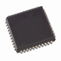
AT89C51RE2-SLSUM Atmel, AT89C51RE2-SLSUM Datasheet - Page 35

AT89C51RE2-SLSUM
Manufacturer Part Number
AT89C51RE2-SLSUM
Description
MCU 8BIT FLASH 2.7-5.5V 44-PLCC
Manufacturer
Atmel
Series
89Cr
Datasheet
1.AT89C51RE2-SLSUM.pdf
(187 pages)
Specifications of AT89C51RE2-SLSUM
Core Processor
8051
Core Size
8-Bit
Speed
60MHz
Connectivity
I²C, SPI, UART/USART
Peripherals
POR, PWM, WDT
Number Of I /o
34
Program Memory Size
128KB (128K x 8)
Program Memory Type
FLASH
Ram Size
8K x 8
Voltage - Supply (vcc/vdd)
2.7 V ~ 5.5 V
Oscillator Type
External
Operating Temperature
-40°C ~ 85°C
Package / Case
44-PLCC
Package
44PLCC
Device Core
8051
Family Name
89C
Maximum Speed
40 MHz
Operating Supply Voltage
3.3|5 V
Data Bus Width
8 Bit
Number Of Programmable I/os
34
Interface Type
SPI/TWI/UART
Number Of Timers
3
Processor Series
AT89x
Core
8051
Data Ram Size
8 KB
Maximum Clock Frequency
40 MHz
Maximum Operating Temperature
+ 85 C
Mounting Style
SMD/SMT
3rd Party Development Tools
PK51, CA51, A51, ULINK2
Development Tools By Supplier
AT89OCD-01
Minimum Operating Temperature
- 40 C
Cpu Family
89C
Device Core Size
8b
Frequency (max)
40MHz
Total Internal Ram Size
8KB
# I/os (max)
34
Number Of Timers - General Purpose
3
Operating Supply Voltage (typ)
3.3/5V
Operating Supply Voltage (max)
5.5V
Operating Supply Voltage (min)
2.7V
Instruction Set Architecture
CISC
Operating Temp Range
-40C to 85C
Operating Temperature Classification
Industrial
Mounting
Surface Mount
Pin Count
44
Package Type
PLCC
For Use With
AT89OCD-01 - USB EMULATOR FOR AT8XC51 MCUAT89STK-11 - KIT STARTER FOR AT89C51RX2
Lead Free Status / RoHS Status
Lead free / RoHS Compliant
Eeprom Size
-
Data Converters
-
Lead Free Status / Rohs Status
Lead free / RoHS Compliant
Available stocks
Company
Part Number
Manufacturer
Quantity
Price
Company:
Part Number:
AT89C51RE2-SLSUM
Manufacturer:
HONEYWELL
Quantity:
101
Column latches
Cross Memory Access
Description overview
7663E–8051–10/08
The column latches, also part of FM0, has a size of one page (128 bytes).
The column latches are the entrance buffers of the three previous memory locations (user array,
XROW, Hardware security byte and Fuse Configuration Byte).
This block is write only from FM0, RM0.
The FM0 memory can be programmed from RM0 without entering idle mode.
Programming FM0 from FM0 makes the CPU core entering “pseudo idle” mode.
In the pseudo idle mode, the code execution is halted, the peripherals are still running (like stan-
dard idle mode) but all interrupt are delayed to the end of this mode. There are fours ways of
exiting pseudo idle mode:
•
•
•
•
Programming FM0 from external memory code (EA=0 or EA=1,with Bank3 active) is impossible.
If a reset occurs during flash programming the target page could be incompletely erased or pro-
grammed, but any other memory location (FM0, RAM, XRAM) remain unchanged.
The Table 21 shows all software flash access allowed.
Table 21. Cross Memory Access
1.
N.A. Not applicable
At the end of the regular flash programming operation
Reset the chip by external reset
Reset the chip by hardware watchdog
Reset the chip by PCA watchdog
External memory
Depends of general lock bits configuration
EA=1, Bank3
(user Flash)
(boot ROM)
EA = 0
RM0
FM0
or
Load column latch
Load column latch
Load column latch
Action
Read
Read
Read
Write
Write
Write
ok (pseudo idle mode)
(user Flash)
Denied
Denied
FM0
ok
ok
ok
ok
ok
(1)
AT89C51RE2
(boot ROM)
Denied
Denied
RM0
N.A.
N.A.
N.A.
N.A.
N.A.
N.A.
ok
35


