AT91SAM9R64-CU Atmel, AT91SAM9R64-CU Datasheet - Page 828
AT91SAM9R64-CU
Manufacturer Part Number
AT91SAM9R64-CU
Description
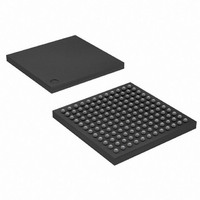
MCU ARM9 64K SRAM 144-LFBGA
Manufacturer
Atmel
Series
AT91SAMr
Specifications of AT91SAM9R64-CU
Core Processor
ARM9
Core Size
16/32-Bit
Speed
240MHz
Connectivity
EBI/EMI, I²C, MMC, SPI, SSC, UART/USART, USB
Peripherals
AC'97, POR, PWM, WDT
Number Of I /o
49
Program Memory Size
32KB (32K x 8)
Program Memory Type
ROM
Ram Size
72K x 8
Voltage - Supply (vcc/vdd)
1.08 V ~ 1.32 V
Data Converters
A/D 3x10b
Oscillator Type
Internal
Operating Temperature
-40°C ~ 85°C
Package / Case
144-LFBGA
Processor Series
AT91SAMx
Core
ARM926EJ-S
Data Bus Width
32 bit
Data Ram Size
64 KB
Interface Type
2-Wire, SPI, SSC, USART
Maximum Clock Frequency
240 MHz
Number Of Programmable I/os
118
Number Of Timers
4
Maximum Operating Temperature
+ 85 C
Mounting Style
SMD/SMT
3rd Party Development Tools
JTRACE-ARM-2M, MDK-ARM, RL-ARM, ULINK2
Development Tools By Supplier
AT91SAM-ICE, AT91-ISP, AT91SAM9RL-EK
Minimum Operating Temperature
- 40 C
On-chip Adc
10 bit, 3 Channel
Controller Family/series
AT91SAM9xxx
No. Of I/o's
49
Ram Memory Size
64KB
Cpu Speed
240MHz
No. Of Timers
3
Rohs Compliant
Yes
Package
144LFBGA
Device Core
ARM926EJ-S
Family Name
91S
Maximum Speed
240 MHz
Operating Supply Voltage
1.8|3.3 V
For Use With
AT91SAM-ICE - EMULATOR FOR AT91 ARM7/ARM9
Lead Free Status / RoHS Status
Lead free / RoHS Compliant
Eeprom Size
-
Lead Free Status / Rohs Status
Lead free / RoHS Compliant
Available stocks
Company
Part Number
Manufacturer
Quantity
Price

Part Number:
AT91SAM9R64-CU
Manufacturer:
ATMEL/爱特梅尔
Quantity:
20 000


43.5
43.5.1
43.5.2
43.5.3
43.5.4
828
Analog-to-digital Converter Functional Description
AT91SAM9R64/RL64 Preliminary
ADC Resolution
ADC Clock
Sleep Mode
Startup Time
The TSADCC embeds a Successive Approximation Register (SAR) Analog-to-Digital Converter
(ADC). The ADC supports 8-bit or 10-bit resolutions.
The conversion is performed on a full range between 0V and the reference voltage pin TSAD-
VREF. Analog inputs between these voltages convert to values based on a linear conversion.
The ADC supports 8-bit or 10-bit resolutions. The 8-bit selection is performed by setting the bit
LOWRES in the TSADCC Mode Register. See
page
By default, after a reset, the resolution is the highest and the DATA field in the
nel Data Register x (x = 0..5)”
By setting the bit LOWRES, the ADC switches in the lowest resolution and the conversion
results can be read in the eight lowest significant bits of the data registers. The two highest bits
of the DATA field in the corresponding TSADCC_CDR register and of the LDATA field in the
TSADCC_LCDR register read 0.
Moreover, when a PDC channel is connected to the TSADCC, 10-bit resolution sets the transfer
request sizes to 16-bit. Setting the bit LOWRES automatically switches to 8-bit data transfers. In
this case, the destination buffers are optimized.
All the conversions for the Touch Screen forces the ADC in 10-bit resolution, regardless of the
LOWRES setting. Further details are given in the section
The TSADCC uses the ADC Clock to perform conversions. Converting a single analog value to
a 10-bit digital data requires Sample and Hold Clock cycles as defined in the field SHTIM of the
“TSADCC Mode Register”
the PRESCAL field of the
The ADC clock range is between MCK/2, if PRESCAL is 0, and MCK/128, if PRESCAL is set to
63 (0x3F). PRESCAL must be programmed in order to provide an ADC clock frequency accord-
ing to the maximum sampling rate parameter given in the Electrical Characteristics section.
The TSADCC Sleep Mode maximizes power saving by automatically deactivating the Analog-to-
Digital Converter cell when it is not being used for conversions. Sleep Mode is enabled by set-
ting the bit SLEEP in
The SLEEP of the ADC is automatically managed by the conversion sequencer, which can auto-
matically process the conversions of all channels at lowest power consumption.
When a trigger occurs, the Analog-to-Digital Converter cell is automatically activated. As the
analog cell requires a start-up time, the logic waits during this time and then starts the conver-
sion on the enabled channels. When all conversions are complete, the ADC is deactivated until
the next trigger.
The Touch Screen ADC has a minimal Startup Time when it exits the Sleep Mode. As the ADC
Clock depends on the application, the user has to program the field STARTUP in the
840.
“TSADCC Mode
“TSADCC Mode
and 10 ADC Clock cycles. The ADC Clock frequency is selected in
are fully used.
Register”.
Register”.
Section 43.10.2 “TSADCC Mode Register” on
“Operating Modes” on page
6289C–ATARM–28-May-09
“TSADCC Chan-
835.
“TSADCC
Related parts for AT91SAM9R64-CU
Image
Part Number
Description
Manufacturer
Datasheet
Request
R

Part Number:
Description:
MCU, MPU & DSP Development Tools KICKSTART KIT FOR AT91SAM9 PLUS
Manufacturer:
IAR Systems

Part Number:
Description:
DEV KIT FOR AVR/AVR32
Manufacturer:
Atmel
Datasheet:

Part Number:
Description:
INTERVAL AND WIPE/WASH WIPER CONTROL IC WITH DELAY
Manufacturer:
ATMEL Corporation
Datasheet:
Part Number:
Description:
Low-Voltage Voice-Switched IC for Hands-Free Operation
Manufacturer:
ATMEL Corporation
Datasheet:
Part Number:
Description:
MONOLITHIC INTEGRATED FEATUREPHONE CIRCUIT
Manufacturer:
ATMEL Corporation
Datasheet:
Part Number:
Description:
AM-FM Receiver IC U4255BM-M
Manufacturer:
ATMEL Corporation
Datasheet:
Part Number:
Description:
Monolithic Integrated Feature Phone Circuit
Manufacturer:
ATMEL Corporation
Datasheet:
Part Number:
Description:
Multistandard Video-IF and Quasi Parallel Sound Processing
Manufacturer:
ATMEL Corporation
Datasheet:
Part Number:
Description:
High-performance EE PLD
Manufacturer:
ATMEL Corporation
Datasheet:
Part Number:
Description:
8-bit Flash Microcontroller
Manufacturer:
ATMEL Corporation
Datasheet:
Part Number:
Description:
2-Wire Serial EEPROM
Manufacturer:
ATMEL Corporation
Datasheet: