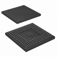
AT91SAM9261B-CU Atmel, AT91SAM9261B-CU Datasheet - Page 20

AT91SAM9261B-CU
Manufacturer Part Number
AT91SAM9261B-CU
Description
MCU ARM9 ULTRA LOW PWR 217-LFBGA
Manufacturer
Atmel
Series
AT91SAMr
Datasheet
1.AT91SAM9261B-CU.pdf
(44 pages)
Specifications of AT91SAM9261B-CU
Core Processor
ARM9
Core Size
16/32-Bit
Speed
190MHz
Connectivity
EBI/EMI, I²C, MMC, SPI, SSC, UART/USART, USB
Peripherals
DMA, LCD, POR, PWM, WDT
Number Of I /o
96
Program Memory Size
32KB (32K x 8)
Program Memory Type
ROM
Ram Size
192K x 8
Voltage - Supply (vcc/vdd)
1.08 V ~ 1.32 V
Oscillator Type
Internal
Operating Temperature
-40°C ~ 85°C
Package / Case
217-LFBGA
Cpu Family
AT91
Device Core
ARM926EJ-S
Device Core Size
32b
Frequency (max)
240MHz
Total Internal Ram Size
160KB
# I/os (max)
96
Number Of Timers - General Purpose
4
Operating Supply Voltage (typ)
1.2/1.8/3.3V
Operating Supply Voltage (max)
1.32/1.95/3.6V
Operating Supply Voltage (min)
1.08/1.65/2.7/3V
Instruction Set Architecture
RISC
Operating Temp Range
-40C to 85C
Operating Temperature Classification
Industrial
Mounting
Surface Mount
Pin Count
217
Package Type
LFBGA
Processor Series
AT91SAMx
Core
ARM926EJ-S
Data Bus Width
32 bit
Data Ram Size
160 KB
Interface Type
JTAG,SPI, SSC, TWI, UART
Maximum Clock Frequency
190 MHz
Number Of Programmable I/os
96
Number Of Timers
3
Operating Supply Voltage
3 V to 3.6 V
Maximum Operating Temperature
+ 85 C
Mounting Style
SMD/SMT
3rd Party Development Tools
JTRACE-ARM-2M, MDK-ARM, RL-ARM, ULINK2
Development Tools By Supplier
AT91SAM-ICE, AT91-ISP, AT91SAM9261-EK
Minimum Operating Temperature
- 40 C
Controller Family/series
AT91SAM9xxx
No. Of I/o's
96
Ram Memory Size
160KB
Cpu Speed
190MHz
No. Of Timers
1
Rohs Compliant
Yes
For Use With
AT91SAM9261-EK - KIT EVAL FOR AT91SAM926EJ-S
Lead Free Status / RoHS Status
Lead free / RoHS Compliant
Eeprom Size
-
Data Converters
-
Lead Free Status / Rohs Status
Compliant
Available stocks
Company
Part Number
Manufacturer
Quantity
Price
Company:
Part Number:
AT91SAM9261B-CU
Manufacturer:
Atmel
Quantity:
126
Company:
Part Number:
AT91SAM9261B-CU
Manufacturer:
ATMEL
Quantity:
5 000
Part Number:
AT91SAM9261B-CU
Manufacturer:
ATMEL/爱特梅尔
Quantity:
20 000
8.1.2
8.1.2.1
8.1.2.2
20
AT91SAM9261 Preliminary
Boot Strategies
BMS = 1, Boot on Embedded ROM
BMS = 0, Boot on External Memory
The system always boots at address 0x0. To ensure a maximum number of possibilities for boot,
the memory layout can be configured with two parameters.
REMAP allows the user to lay out the first internal SRAM bank to 0x0 to ease development. This
is done by software once the system has booted for each Master of the Bus Matrix. Refer to the
Bus Matrix Section for more details.
When REMAP = 0, BMS allows the user to lay out to 0x0, at his convenience, the ROM or an
external memory. This is done via hardware at reset.
Note:
The AT91SAM9261 Bus Matrix manages a boot memory that depends on the level on the BMS
pin at reset. The internal memory area mapped between address 0x0 and 0x000F FFFF is
reserved for this purpose.
If BMS is detected at 1, the boot memory is the embedded ROM.
If BMS is detected at 0, the boot memory is the memory connected on the Chip Select 0 of the
External Bus Interface.
The system boots using the Boot Program.
The customer-programmed software must perform a complete configuration.
To speed up the boot sequence when booting at 32 kHz EBI CS0 (BMS=0), the user must take
the following steps:
• Downloads and runs an application from external storage media into internal SRAM
• Downloaded code size depends on embedded SRAM size
• Automatic detection of valid application
• Bootloader on a non-volatile memory
• SAM-BA
• Boot on slow clock (32,768 Hz)
• Boot with the default configuration for the Static Memory Controller, byte select mode, 16-bit
1. Program the PMC (main oscillator enable or bypass mode).
2. Program and start the PLL.
3. Reprogram the SMC setup, cycle, hold, mode timings registers for CS0 to adapt them
4. Switch the main clock to the new value.
data bus, Read/Write controlled by Chip Select, allows boot on 16-bit non-volatile memory.
– SDCard
– NAND Flash
– SPI DataFlash connected on NPCS0 of the SPI
– Serial communication on a DBGU
– USB Device HS Port
to the new clock
Memory blocks not affected by these parameters can always be seen at their specified base
addresses. See the complete memory map presented in
®
boot in case no valid program is detected in external NVM, supporting:
Figure 8-1 on page
6062LS–ATARM–23-Mar-09
16.


