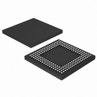
LPC3131FET180,551 NXP Semiconductors, LPC3131FET180,551 Datasheet - Page 15

LPC3131FET180,551
Manufacturer Part Number
LPC3131FET180,551
Description
IC ARM9 MCU 180MHZ 180-TFBGA
Manufacturer
NXP Semiconductors
Series
LPC3000r
Datasheet
1.OM11024.pdf
(72 pages)
Specifications of LPC3131FET180,551
Package / Case
180-TFBGA
Core Processor
ARM9
Core Size
32-Bit
Speed
180MHz
Connectivity
EBI/EMI, I²C, MMC, SPI, UART/USART, USB OTG
Peripherals
DMA, I²S, LCD, PWM, WDT
Program Memory Type
ROMless
Ram Size
192K x 8
Voltage - Supply (vcc/vdd)
1.1 V ~ 3.6 V
Data Converters
A/D 4x10b
Oscillator Type
External
Operating Temperature
-40°C ~ 85°C
Processor Series
LPC31
Core
ARM926EJ-S
Data Bus Width
16 bit, 32 bit
Data Ram Size
192 KB
Interface Type
I2C/I2S/UART/USB
Maximum Clock Frequency
180 MHz
Number Of Timers
4
Operating Supply Voltage
2.7 V to 3.6 V
Maximum Operating Temperature
+ 85 C
Mounting Style
SMD/SMT
3rd Party Development Tools
MDK-ARM, RL-ARM, ULINK2, KSK-LPC3131-PL
Development Tools By Supplier
OM11028
Minimum Operating Temperature
- 40 C
On-chip Adc
4-ch x 10-bit
Lead Free Status / RoHS Status
Lead free / RoHS Compliant
For Use With
568-4850 - KIT EVAL FOR LPC313X568-4062 - DEBUGGER J-LINK JTAG568-4061 - DEBUGGER U-LINK2 JTAG FOR NXP
Number Of I /o
-
Eeprom Size
-
Program Memory Size
-
Lead Free Status / Rohs Status
Lead free / RoHS Compliant
Other names
568-4697
935288014551
LPC3131FET180-S
935288014551
LPC3131FET180-S
Available stocks
Company
Part Number
Manufacturer
Quantity
Price
Company:
Part Number:
LPC3131FET180,551
Manufacturer:
NXP Semiconductors
Quantity:
10 000
NXP Semiconductors
LPC3130_3131
Preliminary data sheet
6.3 JTAG
6.4 NAND flash controller
The Joint Test Action Group (JTAG) interface allows the incorporation of the
LPC3130/3131 in a JTAG scan chain.
This module has the following features:
The NAND flash controller is used as a dedicated interface to NAND flash devices.
Figure 4
module is formed by a controller block that controls the flow of data from/to the AHB bus
through the NAND flash controller block to/from the (external) NAND flash. An error
correction encoder/decoder (ECC enc/dec) module allows for hardware error correction
for support of Multi-Level Cell (MLC) NAND flash devices.
Before data is written from the buffer to the NAND flash, optionally it is first protected by
an error correction code generated by the ECC module. After data is read from the NAND
flash, the error correction module corrects any errors.
This module has the following features:
Fig 4. Block diagram of the NAND flash controller
•
•
•
•
•
ARM926 debug access
Boundary scan
Dedicated NAND flash interface with hardware controlled read and write accesses.
Wear leveling support with 516 byte mode.
Software controlled command and address transfers to support wide range of flash
devices.
shows a block diagram of the NAND flash controller module. The heart of the
All information provided in this document is subject to legal disclaimers.
Rev. 1.04 — 27 May 2010
AHB MULTILAYER MATRIX
NAND INTERFACE
CONTROLLER
Low-cost, low-power ARM926EJ-S microcontrollers
BUFFER
ENCODER/
DECODER
ECC
DMA transfer request
LPC3130/3131
002aae127
© NXP B.V. 2010. All rights reserved.
15 of 72


