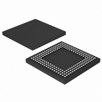
LPC3131FET180,551 NXP Semiconductors, LPC3131FET180,551 Datasheet - Page 8

LPC3131FET180,551
Manufacturer Part Number
LPC3131FET180,551
Description
IC ARM9 MCU 180MHZ 180-TFBGA
Manufacturer
NXP Semiconductors
Series
LPC3000r
Datasheet
1.OM11024.pdf
(72 pages)
Specifications of LPC3131FET180,551
Package / Case
180-TFBGA
Core Processor
ARM9
Core Size
32-Bit
Speed
180MHz
Connectivity
EBI/EMI, I²C, MMC, SPI, UART/USART, USB OTG
Peripherals
DMA, I²S, LCD, PWM, WDT
Program Memory Type
ROMless
Ram Size
192K x 8
Voltage - Supply (vcc/vdd)
1.1 V ~ 3.6 V
Data Converters
A/D 4x10b
Oscillator Type
External
Operating Temperature
-40°C ~ 85°C
Processor Series
LPC31
Core
ARM926EJ-S
Data Bus Width
16 bit, 32 bit
Data Ram Size
192 KB
Interface Type
I2C/I2S/UART/USB
Maximum Clock Frequency
180 MHz
Number Of Timers
4
Operating Supply Voltage
2.7 V to 3.6 V
Maximum Operating Temperature
+ 85 C
Mounting Style
SMD/SMT
3rd Party Development Tools
MDK-ARM, RL-ARM, ULINK2, KSK-LPC3131-PL
Development Tools By Supplier
OM11028
Minimum Operating Temperature
- 40 C
On-chip Adc
4-ch x 10-bit
Lead Free Status / RoHS Status
Lead free / RoHS Compliant
For Use With
568-4850 - KIT EVAL FOR LPC313X568-4062 - DEBUGGER J-LINK JTAG568-4061 - DEBUGGER U-LINK2 JTAG FOR NXP
Number Of I /o
-
Eeprom Size
-
Program Memory Size
-
Lead Free Status / Rohs Status
Lead free / RoHS Compliant
Other names
568-4697
935288014551
LPC3131FET180-S
935288014551
LPC3131FET180-S
Available stocks
Company
Part Number
Manufacturer
Quantity
Price
Company:
Part Number:
LPC3131FET180,551
Manufacturer:
NXP Semiconductors
Quantity:
10 000
NXP Semiconductors
Table 4.
Pin names with prefix m are multiplexed pins. See
LPC3130_3131
Preliminary data sheet
Pin name
Serial Peripheral Interface
SPI_CS_OUT0
SPI_SCK
SPI_MISO
SPI_MOSI
SPI_CS_IN
Digital power supply
VDDI
VSSI
Peripheral power supply
VDDE_IOA
VDDE_IOB
VDDE_IOC
VSSE_IOA
[4]
[4]
[4]
Pin description
[4]
[4]
BGA
ball
A7
A8
C8
B7
B8
H3;
L7;
L12;
C12;
C6;
A9;
C9
A11;
C7;
D12;
G4;
L6;
L11
B2;
E5;
F5;
G5;
H5
L4;
M5;
M7;
M9
C13;
D5;
D7;
E8;
G12;
L10;
K11
C3;
C4;
E4;
F4;
H4;
K3
Digital
I/O
level
[1]
SUP3
SUP3
SUP3
SUP3
SUP3
SUP1
SUP4
SUP8
SUP3
All information provided in this document is subject to legal disclaimers.
Application
function
DO
DIO
DIO
DIO
DI
Supply
Ground
Supply
Supply
Supply
Ground
Rev. 1.04 — 27 May 2010
Table 10
Pin
state
after
reset
O
I
I
I
I
-
-
-
-
-
-
for pin function selection of multiplexed pins.
Low-cost, low-power ARM926EJ-S microcontrollers
[2]
Cell type
[3]
DIO4
DIO4
DIO4
DIO4
DIO4
CS2
CG2
PS1
PS1
PS1
PG1
Description
SPI Chip Select Output (Master)
SPI Clock Input (Slave) / Clock Output
(Master)
SPI Data Input (Master) / Data Output (Slave)
SPI Data Output (Master) / Data Input (Slave)
SPI Chip Select Input (Slave)
Digital Core Supply
Digital Core Ground
Peripheral supply for NAND flash interface
Peripheral supply for SDRAM/LCD
Peripheral supply
LPC3130/3131
© NXP B.V. 2010. All rights reserved.
8 of 72


