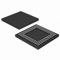
LPC3131FET180,551 NXP Semiconductors, LPC3131FET180,551 Datasheet - Page 27

LPC3131FET180,551
Manufacturer Part Number
LPC3131FET180,551
Description
IC ARM9 MCU 180MHZ 180-TFBGA
Manufacturer
NXP Semiconductors
Series
LPC3000r
Datasheet
1.OM11024.pdf
(72 pages)
Specifications of LPC3131FET180,551
Package / Case
180-TFBGA
Core Processor
ARM9
Core Size
32-Bit
Speed
180MHz
Connectivity
EBI/EMI, I²C, MMC, SPI, UART/USART, USB OTG
Peripherals
DMA, I²S, LCD, PWM, WDT
Program Memory Type
ROMless
Ram Size
192K x 8
Voltage - Supply (vcc/vdd)
1.1 V ~ 3.6 V
Data Converters
A/D 4x10b
Oscillator Type
External
Operating Temperature
-40°C ~ 85°C
Processor Series
LPC31
Core
ARM926EJ-S
Data Bus Width
16 bit, 32 bit
Data Ram Size
192 KB
Interface Type
I2C/I2S/UART/USB
Maximum Clock Frequency
180 MHz
Number Of Timers
4
Operating Supply Voltage
2.7 V to 3.6 V
Maximum Operating Temperature
+ 85 C
Mounting Style
SMD/SMT
3rd Party Development Tools
MDK-ARM, RL-ARM, ULINK2, KSK-LPC3131-PL
Development Tools By Supplier
OM11028
Minimum Operating Temperature
- 40 C
On-chip Adc
4-ch x 10-bit
Lead Free Status / RoHS Status
Lead free / RoHS Compliant
For Use With
568-4850 - KIT EVAL FOR LPC313X568-4062 - DEBUGGER J-LINK JTAG568-4061 - DEBUGGER U-LINK2 JTAG FOR NXP
Number Of I /o
-
Eeprom Size
-
Program Memory Size
-
Lead Free Status / Rohs Status
Lead free / RoHS Compliant
Other names
568-4697
935288014551
LPC3131FET180-S
935288014551
LPC3131FET180-S
Available stocks
Company
Part Number
Manufacturer
Quantity
Price
Company:
Part Number:
LPC3131FET180,551
Manufacturer:
NXP Semiconductors
Quantity:
10 000
NXP Semiconductors
LPC3130_3131
Preliminary data sheet
6.19 Event router
The event router extends the interrupt capability of the system by offering a flexible and
versatile way of generating interrupts. Combined with the wake-up functionality of the
CGU, it also offers a way to wake up the system from suspend mode (with all clocks
deactivated).
The event router has four interrupt outputs connected to the interrupt controller and one
wake-up output connected to the CGU as shown in
activated when an event (for instance a rising edge) is detected on one of the input
signals. The input signals of the event router are connected to relevant internal control
signals in the system or to external signals through pins of the LPC3130/3131.
This module has the following features:
Remark: All pins that can be used as GPIO are connected to the event router (see
Figure
in GPIO mode.
Fig 8. Event router block diagram
•
•
•
•
•
•
•
•
•
•
•
Provides programmable routing of input events to multiple outputs for use as
interrupts or wake up signals.
Input events can come from internal signals or from the pins that can be used as
GPIO.
Inputs can be used either directly or latched (edge detected) as an event source.
The active level (polarity) of the input signal for triggering events is programmable.
Direct events will disappear when the input becomes inactive.
Latched events will remain active until they are explicitly cleared.
Each input can be masked globally for all inputs at once.
Each input can be masked for each output individually.
Event detect status can be read for each output separately.
Event detection is fully asynchronous (no active clock required).
Module can be used to generate a system wake-up from suspend mode.
8). Note that they can be used to trigger events when in normal functional mode or
All information provided in this document is subject to legal disclaimers.
APB
Rev. 1.04 — 27 May 2010
input signals
internal
EVENT ROUTER
Low-cost, low-power ARM926EJ-S microcontrollers
(GPIO configurable)
external pins
cgu wakeup
interrupt 0
interrupt 1
interrupt 2
interrupt 3
Figure
8. The output signals are
LPC3130/3131
CONTROLLER
INTERRUPT
CGU
002aae087
© NXP B.V. 2010. All rights reserved.
27 of 72


