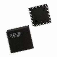
PXAG30KBA,512 NXP Semiconductors, PXAG30KBA,512 Datasheet - Page 16

PXAG30KBA,512
Manufacturer Part Number
PXAG30KBA,512
Description
IC XA MCU 16BIT ROMLESS 44-PLCC
Manufacturer
NXP Semiconductors
Series
XAr
Datasheet
1.PXAG30KBBD157.pdf
(36 pages)
Specifications of PXAG30KBA,512
Core Processor
XA
Core Size
16-Bit
Speed
30MHz
Connectivity
UART/USART
Peripherals
PWM, WDT
Number Of I /o
32
Program Memory Type
ROMless
Ram Size
512 x 8
Voltage - Supply (vcc/vdd)
2.7 V ~ 5.5 V
Oscillator Type
External
Operating Temperature
0°C ~ 70°C
Package / Case
44-PLCC
Processor Series
PXAG3x
Core
80C51
Data Bus Width
16 bit
Data Ram Size
512 B
Interface Type
UART
Maximum Clock Frequency
30 MHz
Number Of Programmable I/os
32
Number Of Timers
3
Operating Supply Voltage
2.7 V to 5.5 V
Maximum Operating Temperature
+ 70 C
Mounting Style
SMD/SMT
Minimum Operating Temperature
0 C
Lead Free Status / RoHS Status
Lead free / RoHS Compliant
Eeprom Size
-
Program Memory Size
-
Data Converters
-
Lead Free Status / Rohs Status
Details
Other names
568-4340-5
935270580512
PXAG30KBA
PXAG30KBA
935270580512
PXAG30KBA
PXAG30KBA
Available stocks
Company
Part Number
Manufacturer
Quantity
Price
Company:
Part Number:
PXAG30KBA,512
Manufacturer:
NXP
Quantity:
800
Company:
Part Number:
PXAG30KBA,512
Manufacturer:
NXP Semiconductors
Quantity:
10 000
independently of the UART itself and provides a start-of-break status
Philips Semiconductors
When the watchdog underflows, the following action takes place
(see Figure 10):
Note that if the watchdog underflows, the program counter will be
loaded from the reset vector as in the case of an internal reset. The
watchdog time-out flag can be examined to determine if the
watchdog has caused the reset condition. The watchdog time-out
flag bit can be cleared by software.
WDCON Register Bit Definitions
WDCON.7
WDCON.6
WDCON.5
WDCON.4
WDCON.3
WDCON.2
WDCON.1
WDCON.0
UARTs
The XA-G30 includes 2 UART ports that are compatible with the
enhanced UART used on the 8xC51FB. Baud rate selection is
somewhat different due to the clocking scheme used for the XA
timers.
Some other enhancements have been made to UART operation.
The first is that there are separate interrupt vectors for each UART’s
transmit and receive functions. The UART transmitter has been
double buffered, allowing packed transmission of data with no gaps
between bytes and less critical interrupt service routine timing. A
break detect function has been added to the UART. This operates
bit that the program may test. Finally, an Overrun Error flag has
been added to detect missed characters in the received data
stream. The double buffered UART transmitter may require some
software changes in code written for the original XA-G30 single
buffered UART.
2002 Mar 25
Autoload takes place.
Watchdog time-out flag is set
Watchdog run bit unchanged.
Autoload (WDL) register unchanged.
Prescaler tap unchanged.
All other device action same as external reset.
XA 16-bit microcontroller family
512 B RAM, watchdog, 2 UARTs
WATCHDOG FEED SEQUENCE
PRE2
PRE1
PRE0
—
—
WDRUN
WDTOF
—
MOV WFEED1,#A5H
MOV WFEED2,#5AH
Prescaler Select 2, reset to 1
Prescaler Select 1, reset to 1
Prescaler Select 0, reset to 1
Watchdog Run Control bit, reset to 1
Timeout flag
TCLK
PRE2
PRESCALER
Figure 10. Watchdog Timer in XA-G30
PRE1
PRE0
14
—
Each UART baud rate is determined by either a fixed division of the
oscillator (in UART modes 0 and 2) or by the timer 1 or timer 2
overflow rate (in UART modes 1 and 3).
Timer 1 defaults to clock both UART0 and UART1. Timer 2 can be
programmed to clock either UART0 through T2CON (via bits R0CLK
and T0CLK) or UART1 through T2MOD (via bits R1CLK and
T1CLK). In this case, the UART not clocked by T2 could use T1 as
the clock source.
The serial port receive and transmit registers are both accessed at
Special Function Register SnBUF. Writing to SnBUF loads the
transmit register, and reading SnBUF accesses a physically
separate receive register.
The serial port can operate in 4 modes:
Mode 0: Serial I/O expansion mode. Serial data enters and exits
through RxDn. TxDn outputs the shift clock. 8 bits are
transmitted/received (LSB first). (The baud rate is fixed at 1/16 the
oscillator frequency.)
Mode 1: Standard 8-bit UART mode. 10 bits are transmitted
(through TxDn) or received (through RxDn): a start bit (0), 8 data
bits (LSB first), and a stop bit (1). On receive, the stop bit goes into
RB8 in Special Function Register SnCON. The baud rate is variable.
Mode 2: Fixed rate 9-bit UART mode. 11 bits are transmitted
(through TxD) or received (through RxD): start bit (0), 8 data bits
(LSB first), a programmable 9th data bit, and a stop bit (1). On
Transmit, the 9th data bit (TB8_n in SnCON) can be assigned the
value of 0 or 1. Or, for example, the parity bit (P, in the PSW) could
be moved into TB8_n. On receive, the 9th data bit goes into RB8_n
in Special Function Register SnCON, while the stop bit is ignored.
The baud rate is programmable to 1/32 of the oscillator frequency.
Mode 3: Standard 9-bit UART mode. 11 bits are transmitted
(through TxDn) or received (through RxDn): a start bit (0), 8 data
bits (LSB first), a programmable 9th data bit, and a stop bit (1).
In fact, Mode 3 is the same as Mode 2 in all respects except baud
rate. The baud rate in Mode 3 is variable.
In all four modes, transmission is initiated by any instruction that
uses SnBUF as a destination register. Reception is initiated in
Mode 0 by the condition RI_n = 0 and REN_n = 1. Reception is
initiated in the other modes by the incoming start bit if REN_n = 1.
—
8–BIT DOWN
COUNTER
WDRUN
WDL
WDTOF
INTERNAL RESET
—
SU00581A
WDCON
XA-G30
Product data


