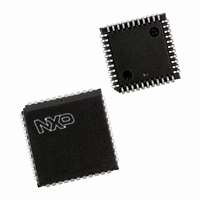
PXAG30KBA,512 NXP Semiconductors, PXAG30KBA,512 Datasheet - Page 25

PXAG30KBA,512
Manufacturer Part Number
PXAG30KBA,512
Description
IC XA MCU 16BIT ROMLESS 44-PLCC
Manufacturer
NXP Semiconductors
Series
XAr
Datasheet
1.PXAG30KBBD157.pdf
(36 pages)
Specifications of PXAG30KBA,512
Core Processor
XA
Core Size
16-Bit
Speed
30MHz
Connectivity
UART/USART
Peripherals
PWM, WDT
Number Of I /o
32
Program Memory Type
ROMless
Ram Size
512 x 8
Voltage - Supply (vcc/vdd)
2.7 V ~ 5.5 V
Oscillator Type
External
Operating Temperature
0°C ~ 70°C
Package / Case
44-PLCC
Processor Series
PXAG3x
Core
80C51
Data Bus Width
16 bit
Data Ram Size
512 B
Interface Type
UART
Maximum Clock Frequency
30 MHz
Number Of Programmable I/os
32
Number Of Timers
3
Operating Supply Voltage
2.7 V to 5.5 V
Maximum Operating Temperature
+ 70 C
Mounting Style
SMD/SMT
Minimum Operating Temperature
0 C
Lead Free Status / RoHS Status
Lead free / RoHS Compliant
Eeprom Size
-
Program Memory Size
-
Data Converters
-
Lead Free Status / Rohs Status
Details
Other names
568-4340-5
935270580512
PXAG30KBA
PXAG30KBA
935270580512
PXAG30KBA
PXAG30KBA
Available stocks
Company
Part Number
Manufacturer
Quantity
Price
Company:
Part Number:
PXAG30KBA,512
Manufacturer:
NXP
Quantity:
800
Company:
Part Number:
PXAG30KBA,512
Manufacturer:
NXP Semiconductors
Quantity:
10 000
1. Load capacitance for all outputs = 80 pF.
2. Variables V1 through V13 reflect programmable bus timing, which is programmed via the Bus Timing registers (BTRH and BTRL).
Philips Semiconductors
AC ELECTRICAL CHARACTERISTICS (V
T
NOTES:
2002 Mar 25
amb
Address Cycle
Code Read Cycle
Data Read Cycle
Data Write Cycle
Wait Input
SYMBOL
SYMBOL
XA 16-bit microcontroller family
512 B RAM, watchdog, 2 UARTs
t
t
t
t
t
t
t
t
t
t
t
t
t
t
t
t
t
t
t
t
t
t
t
t
t
t
t
t
CRAR
LHLL
AVLL
LLAX
PLPH
LLPL
AVIVA
AVIVB
PLIV
PXIX
PXIZ
IXUA
RLRH
LLRL
AVDVA
AVDVB
RLDV
RHDX
RHDZ
DXUA
WLWH
LLWL
QVWX
WHQX
AVWL
UAWH
WTH
WTL
Refer to the XA User Guide for details of the bus timing settings.
V1)
V2)
= 0 to +70 C for commercial, –40 C to +85 C for industrial.
V1 = 0.5 if the ALEW bit = 0, and 1.5 if the ALEW bit = 1.
ALEW bits in the BTRL register.
– For a bus cycle with no ALE, V2 = 1 if CR1/0 = 00, 2 if CR1/0 = 01, 3 if CR1/0 = 10, and 4 if CR1/0 = 11. Note that during burst
– For a bus cycle with an ALE, V2 = the total bus cycle duration (2 if CRA1/0 = 00, 3 if CRA1/0 = 01, 4 if CRA1/0 = 10,
This variable represents the programmed width of the ALE pulse as determined by the ALEW bit in the BTRL register.
This variable represents the programmed width of the PSEN pulse as determined by the CR1 and CR0 bits or the CRA1, CRA0, and
mode code fetches, PSEN does not exhibit transitions at the boundaries of bus cycles. V2 still applies for the purpose of
determining peripheral timing requirements.
and 5 if CRA1/0 = 11) minus the number of clocks used by ALE (V1 + 0.5).
Example: If CRA1/0 = 10 and ALEW = 1, the V2 = 4 – (1.5 + 0.5) = 2.
FIGURE
FIGURE
21
16
16
16
16
16
16
17
16
16
16
16
18
18
18
19
18
18
18
18
20
20
20
20
20
20
21
21
Delay from clock rising edge to ALE rising edge
ALE pulse width (programmable)
Address valid to ALE de-asserted (set-up)
Address hold after ALE de-asserted
PSEN pulse width
ALE de-asserted to PSEN asserted
Address valid to instruction valid, ALE cycle (access time)
Address valid to instruction valid, non-ALE cycle (access time)
PSEN asserted to instruction valid (enable time)
Instruction hold after PSEN de-asserted
Bus 3-State after PSEN de-asserted (disable time)
Hold time of unlatched part of address after instruction latched
RD pulse width
ALE de-asserted to RD asserted
Address valid to data input valid, ALE cycle (access time)
Address valid to data input valid, non-ALE cycle (access time)
RD low to valid data in, enable time
Data hold time after RD de-asserted
Bus 3-State after RD de-asserted (disable time)
Hold time of unlatched part of address after data latched
WR pulse width
ALE falling edge to WR asserted
Data valid before WR asserted (data setup time)
Data hold time after WR de-asserted (Note 6)
Address valid to WR asserted (address setup time) (Note 5)
Hold time of unlatched part of address after WR is de-asserted
WAIT stable after bus strobe (RD, WR, or PSEN) asserted
WAIT hold after bus strobe (RD, WR, or PSEN) assertion
DD
PARAMETER
PARAMETER
= 2.7 V to 4.5 V)
23
(V12 * t
(V13 * t
(V11 * t
(V1 * t
(V1 * t
(V2 * t
(V7 * t
(V8 * t
(V9 * t
(V10 * t
(V11 * t
(t
(t
(t
C
C
C
/2) – 12
MIN
/2) – 9
/2) – 9
VARIABLE CLOCK
15
0
0
0
0
C
C
C
C
C
C
C
C
C
C
) – 10
) – 18
) – 12
) – 12
) – 12
) – 28
C
) – 10
) – 10
) – 28
) – 8
) – 5
(V10 * t
(V3 * t
(V4 * t
(V2 * t
(V6 * t
(V5 * t
(V7 * t
t
t
MAX
C
C
60
C
C
C
– 8
C
C
C
– 8
C
) – 58
) – 52
) – 52
) – 58
) – 52
) – 52
) – 40
XA-G30
Product data
UNIT
UNIT
ns
ns
ns
ns
ns
ns
ns
ns
ns
ns
ns
ns
ns
ns
ns
ns
ns
ns
ns
ns
ns
ns
ns
ns
ns
ns
ns
ns


