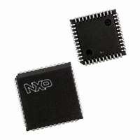
PXAG30KBA,512 NXP Semiconductors, PXAG30KBA,512 Datasheet - Page 20

PXAG30KBA,512
Manufacturer Part Number
PXAG30KBA,512
Description
IC XA MCU 16BIT ROMLESS 44-PLCC
Manufacturer
NXP Semiconductors
Series
XAr
Datasheet
1.PXAG30KBBD157.pdf
(36 pages)
Specifications of PXAG30KBA,512
Core Processor
XA
Core Size
16-Bit
Speed
30MHz
Connectivity
UART/USART
Peripherals
PWM, WDT
Number Of I /o
32
Program Memory Type
ROMless
Ram Size
512 x 8
Voltage - Supply (vcc/vdd)
2.7 V ~ 5.5 V
Oscillator Type
External
Operating Temperature
0°C ~ 70°C
Package / Case
44-PLCC
Processor Series
PXAG3x
Core
80C51
Data Bus Width
16 bit
Data Ram Size
512 B
Interface Type
UART
Maximum Clock Frequency
30 MHz
Number Of Programmable I/os
32
Number Of Timers
3
Operating Supply Voltage
2.7 V to 5.5 V
Maximum Operating Temperature
+ 70 C
Mounting Style
SMD/SMT
Minimum Operating Temperature
0 C
Lead Free Status / RoHS Status
Lead free / RoHS Compliant
Eeprom Size
-
Program Memory Size
-
Data Converters
-
Lead Free Status / Rohs Status
Details
Other names
568-4340-5
935270580512
PXAG30KBA
PXAG30KBA
935270580512
PXAG30KBA
PXAG30KBA
Available stocks
Company
Part Number
Manufacturer
Quantity
Price
Company:
Part Number:
PXAG30KBA,512
Manufacturer:
NXP
Quantity:
800
Company:
Part Number:
PXAG30KBA,512
Manufacturer:
NXP Semiconductors
Quantity:
10 000
Philips Semiconductors
2002 Mar 25
XA 16-bit microcontroller family
512 B RAM, watchdog, 2 UARTs
SnCON
Bit Addressable
Reset Value: 00H
BIT
SnCON.5 SM2
SnCON.4 REN
SnCON.3 TB8
SnCON.2 RB8
SnCON.1 TI
SnCON.0 RI
Address:
SYMBOL FUNCTION
S0CON 420
S1CON 424
Enables the multiprocessor communication feature in Modes 2 and 3. In Mode 2 or 3, if SM2 is set to 1, then RI
will not be activated if the received 9th data bit (RB8) is 0. In Mode 1, if SM2=1 then RI will not be activated if a
valid stop bit was not received. In Mode 0, SM2 should be 0.
Enables serial reception. Set by software to enable reception. Clear by software to disable reception.
The 9th data bit that will be transmitted in Modes 2 and 3. Set or clear by software as desired. The TB8 bit is not
double buffered. See text for details.
In Modes 2 and 3, is the 9th data bit that was received. In Mode 1, if SM2=0, RB8 is the stop bit that was
received. In Mode 0, RB8 is not used.
Transmit interrupt flag. Set when another byte may be written to the UART transmitter. See text for details.
Must be cleared by software.
Receive interrupt flag. Set by hardware at the end of the 8th bit time in Mode 0, or at the end of the stop bit time
in the other modes (except see SM2). Must be cleared by software.
Figure 14. UART Multiprocessor Communication, Automatic Address Recognition
START
BIT
IN UART MODE 2 OR MODE 3 AND SM2 = 1:
– WHEN OWN ADDRESS RECEIVED, CLEAR SM2 TO RECEIVE DATA BYTES
– WHEN ALL DATA BYTES HAVE BEEN RECEIVED: SET SM2 TO WAIT FOR NEXT ADDRESS.
D0
INTERRUPT IF REN=1, RB8=1 AND “RECEIVED ADDRESS” = “PROGRAMMED ADDRESS”
RECEIVED ADDRESS D0 TO D7
Where SM0, SM1 specify the serial port mode, as follows:
—
SM0
PROGRAMMED ADDRESS
D0
0
0
1
1
D1
Figure 12. Serial Port Control (SnCON) Register
—
D1
SM1
Figure 13. UART Framing Error Detection
0
1
0
1
D2
MSB
SM0
SM0_n
—
D2
1
1
Mode
3
D3
0
1
2
SM1
SM1_n
D3
shift register
8-bit UART
9-bit UART
9-bit UART
DATA BYTE
—
Description
1
0
D4
18
SM2
FEn
SM2_n
D4
COMPARATOR
D5
1
REN
D5
REN_n
BRn
Baud Rate
1
f
variable
f
variable
OSC
OSC
D6
/16
/32
D6
TB8
TB8_n
OEn
D7
X
D7
STINTn
RB8
RB8_n
D8
MODE 2, 3
ONLY IN
D8
SnSTAT
TI
TI_n
if 0, sets FE
STOP
BIT
RI_n
RI
LSB
SU00598
XA-G30
SU00613
SnCON
Product data
SU00597C


