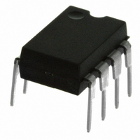
Z8F022APB020SG Zilog, Z8F022APB020SG Datasheet - Page 116
Z8F022APB020SG
Manufacturer Part Number
Z8F022APB020SG
Description
IC ENCORE XP MCU FLASH 2K 8DIP
Manufacturer
Zilog
Series
Encore!® XP®r
Datasheet
1.Z8F08200100KIT.pdf
(264 pages)
Specifications of Z8F022APB020SG
Core Processor
Z8
Core Size
8-Bit
Speed
20MHz
Connectivity
IrDA, UART/USART
Peripherals
Brown-out Detect/Reset, LED, LVD, POR, PWM, Temp Sensor, WDT
Number Of I /o
6
Program Memory Size
2KB (2K x 8)
Program Memory Type
FLASH
Eeprom Size
64 x 8
Ram Size
512 x 8
Voltage - Supply (vcc/vdd)
2.7 V ~ 3.6 V
Data Converters
A/D 4x10b
Oscillator Type
Internal
Operating Temperature
0°C ~ 70°C
Package / Case
8-DIP (0.300", 7.62mm)
Processor Series
Z8F022Ax
Core
eZ8
Data Bus Width
8 bit
Data Ram Size
512 KB
Interface Type
UART
Maximum Clock Frequency
20 MHz
Number Of Programmable I/os
6
Number Of Timers
2
Operating Supply Voltage
2.7 V to 3.6 V
Maximum Operating Temperature
+ 70 C
Mounting Style
Through Hole
Development Tools By Supplier
Z8F04A08100KITG, Z8F04A28100KITG, ZENETSC0100ZACG, ZENETSC0100ZACG, ZUSBOPTSC01ZACG, ZUSBSC00100ZAC, ZUSBSC00100ZACG
Minimum Operating Temperature
0 C
On-chip Adc
10 bit, 4 Channel
Lead Free Status / RoHS Status
Lead free / RoHS Compliant
Other names
269-4089
Z8F022APB020SG
Z8F022APB020SG


Table 56. UART Control 0 Register (U0CTL0)
PS022517-0508
BITS
FIELD
RESET
R/W
ADDR
UART Control 0 and Control 1 Registers
TEN
7
Reserved—Must be 0
NEWFRM—Status bit denoting the start of a new frame. Reading the UART Receive
Data Register resets this bit to 0.
0 = The current byte is not the first data byte of a new frame.
1 = The current byte is the first data byte of a new frame.
MPRX—Multiprocessor Receive
Returns the value of the last multiprocessor bit received. Reading from the UART Receive
Data Register resets this bit to 0.
The UART Control 0 and Control 1 registers
ure the properties of the UART’s transmit and receive operations. The UART Control
Registers must not been written while the UART is enabled.
TEN—Transmit Enable
This bit enables or disables the transmitter. The enable is also controlled by the CTS signal
and the CTSE bit. If the CTS signal is low and the CTSE bit is 1, the transmitter is
enabled.
0 = Transmitter disabled.
1 = Transmitter enabled.
REN—Receive Enable
This bit enables or disables the receiver.
0 = Receiver disabled.
1 = Receiver enabled.
CTSE—CTS Enable
0 = The CTS signal has no effect on the transmitter.
1 = The UART recognizes the CTS signal as an enable control from the transmitter.
PEN—Parity Enable
This bit enables or disables parity. Even or odd is determined by the PSEL bit. This bit is
overridden by the
0 = Parity is disabled.
1 = The transmitter sends data with an additional parity bit and the receiver
receives an additional parity bit.
REN
6
MPEN
CTSE
5
bit.
PEN
4
F42H
R/W
0
PSEL
(Table 56
3
Universal Asynchronous Receiver/Transmitter
and
Z8 Encore! XP
SBRK
2
Table 57
Product Specification
on page 104) config-
STOP
1
®
F0822 Series
LBEN
0
103
Related parts for Z8F022APB020SG
Image
Part Number
Description
Manufacturer
Datasheet
Request
R

Part Number:
Description:
Communication Controllers, ZILOG INTELLIGENT PERIPHERAL CONTROLLER (ZIP)
Manufacturer:
Zilog, Inc.
Datasheet:

Part Number:
Description:
KIT DEV FOR Z8 ENCORE 16K TO 64K
Manufacturer:
Zilog
Datasheet:

Part Number:
Description:
KIT DEV Z8 ENCORE XP 28-PIN
Manufacturer:
Zilog
Datasheet:

Part Number:
Description:
DEV KIT FOR Z8 ENCORE 8K/4K
Manufacturer:
Zilog
Datasheet:

Part Number:
Description:
KIT DEV Z8 ENCORE XP 28-PIN
Manufacturer:
Zilog
Datasheet:

Part Number:
Description:
DEV KIT FOR Z8 ENCORE 4K TO 8K
Manufacturer:
Zilog
Datasheet:
Part Number:
Description:
CMOS Z8 microcontroller. ROM 16 Kbytes, RAM 256 bytes, speed 16 MHz, 32 lines I/O, 3.0V to 5.5V
Manufacturer:
Zilog, Inc.
Datasheet:
Part Number:
Description:
Low-cost microcontroller. 512 bytes ROM, 61 bytes RAM, 8 MHz
Manufacturer:
Zilog, Inc.
Datasheet:
Part Number:
Description:
Z8 4K OTP Microcontroller
Manufacturer:
Zilog, Inc.
Datasheet:
Part Number:
Description:
CMOS SUPER8 ROMLESS MCU
Manufacturer:
Zilog, Inc.
Datasheet:
Part Number:
Description:
SL1866 CMOSZ8 OTP Microcontroller
Manufacturer:
Zilog, Inc.
Datasheet:
Part Number:
Description:
SL1866 CMOSZ8 OTP Microcontroller
Manufacturer:
Zilog, Inc.
Datasheet:
Part Number:
Description:
OTP (KB) = 1, RAM = 125, Speed = 12, I/O = 14, 8-bit Timers = 2, Comm Interfaces Other Features = Por, LV Protect, Voltage = 4.5-5.5V
Manufacturer:
Zilog, Inc.
Datasheet:
Part Number:
Description:
Manufacturer:
Zilog, Inc.
Datasheet: