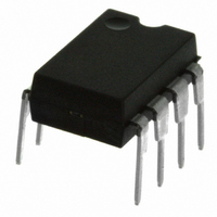
Z8F022APB020SG Zilog, Z8F022APB020SG Datasheet - Page 172

Z8F022APB020SG
Manufacturer Part Number
Z8F022APB020SG
Description
IC ENCORE XP MCU FLASH 2K 8DIP
Manufacturer
Zilog
Series
Encore!® XP®r
Datasheet
1.Z8F08200100KIT.pdf
(264 pages)
Specifications of Z8F022APB020SG
Core Processor
Z8
Core Size
8-Bit
Speed
20MHz
Connectivity
IrDA, UART/USART
Peripherals
Brown-out Detect/Reset, LED, LVD, POR, PWM, Temp Sensor, WDT
Number Of I /o
6
Program Memory Size
2KB (2K x 8)
Program Memory Type
FLASH
Eeprom Size
64 x 8
Ram Size
512 x 8
Voltage - Supply (vcc/vdd)
2.7 V ~ 3.6 V
Data Converters
A/D 4x10b
Oscillator Type
Internal
Operating Temperature
0°C ~ 70°C
Package / Case
8-DIP (0.300", 7.62mm)
Processor Series
Z8F022Ax
Core
eZ8
Data Bus Width
8 bit
Data Ram Size
512 KB
Interface Type
UART
Maximum Clock Frequency
20 MHz
Number Of Programmable I/os
6
Number Of Timers
2
Operating Supply Voltage
2.7 V to 3.6 V
Maximum Operating Temperature
+ 70 C
Mounting Style
Through Hole
Development Tools By Supplier
Z8F04A08100KITG, Z8F04A28100KITG, ZENETSC0100ZACG, ZENETSC0100ZACG, ZUSBOPTSC01ZACG, ZUSBSC00100ZAC, ZUSBSC00100ZACG
Minimum Operating Temperature
0 C
On-chip Adc
10 bit, 4 Channel
Lead Free Status / RoHS Status
Lead free / RoHS Compliant
Other names
269-4089
Z8F022APB020SG
Z8F022APB020SG
- Current page: 172 of 264
- Download datasheet (6Mb)
Table 83. Flash Control Register (FCTL)
Flash Control Register Definitions
PS022517-0508
BITS
FIELD
RESET
R/W
ADDR
Flash Controller Behavior in Debug Mode
Flash Control Register
7
The following changes in behavior of the Flash Controller occur when the Flash Control-
ler is accessed using the OCD:
•
•
•
•
•
•
•
The Flash Control Register
ming and erase operations, or to select the Flash Sector Protect Register. The Write-only
Flash Control Register shares its Register File address with the Read-only Flash Status
Register.
FCMD—Flash Command
73H = First unlock command.
8CH = Second unlock command.
95H = Page erase command.
63H = Mass erase command
5EH = Flash Sector Protect Register select.
* All other commands, or any command out of sequence, lock the Flash Controller.
The Flash Write Protect option bit is ignored
The Flash Sector Protect Register is ignored for programming and erase operations
Programming operations are not limited to the page selected in the Page Select
Register
Bits in the Flash Sector Protect Register can be written to 1 or 0
The second write of the Page Select Register to unlock the Flash Controller is not
necessary
The Page Select Register is written when the Flash Controller is unlocked
The Mass Erase command is enabled
6
5
(Table
83) is used to unlock the Flash Controller for program-
4
FCMD
FF8H
W
0
3
Z8 Encore! XP
2
Product Specification
1
®
F0822 Series
Flash Memory
0
159
Related parts for Z8F022APB020SG
Image
Part Number
Description
Manufacturer
Datasheet
Request
R

Part Number:
Description:
Communication Controllers, ZILOG INTELLIGENT PERIPHERAL CONTROLLER (ZIP)
Manufacturer:
Zilog, Inc.
Datasheet:

Part Number:
Description:
KIT DEV FOR Z8 ENCORE 16K TO 64K
Manufacturer:
Zilog
Datasheet:

Part Number:
Description:
KIT DEV Z8 ENCORE XP 28-PIN
Manufacturer:
Zilog
Datasheet:

Part Number:
Description:
DEV KIT FOR Z8 ENCORE 8K/4K
Manufacturer:
Zilog
Datasheet:

Part Number:
Description:
KIT DEV Z8 ENCORE XP 28-PIN
Manufacturer:
Zilog
Datasheet:

Part Number:
Description:
DEV KIT FOR Z8 ENCORE 4K TO 8K
Manufacturer:
Zilog
Datasheet:

Part Number:
Description:
CMOS Z8 microcontroller. ROM 16 Kbytes, RAM 256 bytes, speed 16 MHz, 32 lines I/O, 3.0V to 5.5V
Manufacturer:
Zilog, Inc.
Datasheet:

Part Number:
Description:
Low-cost microcontroller. 512 bytes ROM, 61 bytes RAM, 8 MHz
Manufacturer:
Zilog, Inc.
Datasheet:

Part Number:
Description:
Z8 4K OTP Microcontroller
Manufacturer:
Zilog, Inc.
Datasheet:

Part Number:
Description:
CMOS SUPER8 ROMLESS MCU
Manufacturer:
Zilog, Inc.
Datasheet:

Part Number:
Description:
SL1866 CMOSZ8 OTP Microcontroller
Manufacturer:
Zilog, Inc.
Datasheet:

Part Number:
Description:
SL1866 CMOSZ8 OTP Microcontroller
Manufacturer:
Zilog, Inc.
Datasheet:

Part Number:
Description:
OTP (KB) = 1, RAM = 125, Speed = 12, I/O = 14, 8-bit Timers = 2, Comm Interfaces Other Features = Por, LV Protect, Voltage = 4.5-5.5V
Manufacturer:
Zilog, Inc.
Datasheet:

Part Number:
Description:
Manufacturer:
Zilog, Inc.
Datasheet:


