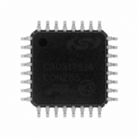
C8051T614-GQ Silicon Laboratories Inc, C8051T614-GQ Datasheet - Page 28

C8051T614-GQ
Manufacturer Part Number
C8051T614-GQ
Description
IC 8051 MCU 8K BYTE-PROG 32-LQFP
Manufacturer
Silicon Laboratories Inc
Series
C8051T61xr
Specifications of C8051T614-GQ
Program Memory Type
OTP
Program Memory Size
8KB (8K x 8)
Package / Case
32-LQFP
Core Processor
8051
Core Size
8-Bit
Speed
25MHz
Connectivity
SMBus (2-Wire/I²C), SPI, UART/USART
Peripherals
POR, PWM, WDT
Number Of I /o
29
Ram Size
1.25K x 8
Voltage - Supply (vcc/vdd)
1.8 V ~ 3.6 V
Oscillator Type
Internal
Operating Temperature
-40°C ~ 85°C
Processor Series
C8051T6x
Core
8051
Data Bus Width
8 bit
Data Ram Size
1.25 KB
Interface Type
I2C/SPI/UART
Maximum Clock Frequency
25 MHz
Number Of Programmable I/os
29
Number Of Timers
4
Maximum Operating Temperature
+ 85 C
Mounting Style
SMD/SMT
3rd Party Development Tools
PK51, CA51, A51, ULINK2
Development Tools By Supplier
C8051FT610DK
Minimum Operating Temperature
- 40 C
On-chip Adc
21-ch x 10-bit
Package
32LQFP
Device Core
8051
Family Name
C8051T61x
Maximum Speed
25 MHz
Operating Supply Voltage
2.5|3.3 V
Lead Free Status / RoHS Status
Lead free / RoHS Compliant
Eeprom Size
-
Data Converters
-
Lead Free Status / Rohs Status
Lead free / RoHS Compliant
Other names
336-1441
Available stocks
Company
Part Number
Manufacturer
Quantity
Price
Company:
Part Number:
C8051T614-GQ
Manufacturer:
Silicon
Quantity:
1 500
Company:
Part Number:
C8051T614-GQ
Manufacturer:
Silicon Laboratories Inc
Quantity:
10 000
Company:
Part Number:
C8051T614-GQR
Manufacturer:
Silicon Laboratories Inc
Quantity:
10 000
C8051T610/1/2/3/4/5/6/7
28
Notes:
General
Solder Mask Design
Stencil Design
Card Assembly
Dimension
1. All dimensions shown are in millimeters (mm) unless otherwise noted.
2. Dimensioning and Tolerancing is per the ANSI Y14.5M-1994 specification.
3. This Land Pattern Design is based on the IPC-7351 guidelines.
4. All metal pads are to be non-solder mask defined (NSMD). Clearance between the solder
5. A stainless steel, laser-cut and electro-polished stencil with trapezoidal walls should be used
6. The stencil thickness should be 0.125mm (5 mils).
7. The ratio of stencil aperture to land pad size should be 1:1 for all perimeter pins.
8. A 3x3 array of 0.90mm openings on a 1.1mm pitch should be used for the center pad to
9. A No-Clean, Type-3 solder paste is recommended.
10. The recommended card reflow profile is per the JEDEC/IPC J-STD-020C specification for
C1
C2
X1
E
mask and the metal pad is to be 60m minimum, all the way around the pad.
to assure good solder paste release.
assure the proper paste volume.
Small Body Components.
Figure 5.2. QFN-28 Recommended PCB Land Pattern
Table 5.2. QFN-28 PCB Land Pattern Dimesions
0.20
Min
4.80
4.80
0.50
Max
0.30
Rev 1.0
Dimension
X2
Y1
Y2
3.20
0.85
3.20
Min
Max
3.30
0.95
3.30


