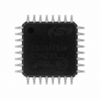
C8051T614-GQ Silicon Laboratories Inc, C8051T614-GQ Datasheet - Page 41

C8051T614-GQ
Manufacturer Part Number
C8051T614-GQ
Description
IC 8051 MCU 8K BYTE-PROG 32-LQFP
Manufacturer
Silicon Laboratories Inc
Series
C8051T61xr
Specifications of C8051T614-GQ
Program Memory Type
OTP
Program Memory Size
8KB (8K x 8)
Package / Case
32-LQFP
Core Processor
8051
Core Size
8-Bit
Speed
25MHz
Connectivity
SMBus (2-Wire/I²C), SPI, UART/USART
Peripherals
POR, PWM, WDT
Number Of I /o
29
Ram Size
1.25K x 8
Voltage - Supply (vcc/vdd)
1.8 V ~ 3.6 V
Oscillator Type
Internal
Operating Temperature
-40°C ~ 85°C
Processor Series
C8051T6x
Core
8051
Data Bus Width
8 bit
Data Ram Size
1.25 KB
Interface Type
I2C/SPI/UART
Maximum Clock Frequency
25 MHz
Number Of Programmable I/os
29
Number Of Timers
4
Maximum Operating Temperature
+ 85 C
Mounting Style
SMD/SMT
3rd Party Development Tools
PK51, CA51, A51, ULINK2
Development Tools By Supplier
C8051FT610DK
Minimum Operating Temperature
- 40 C
On-chip Adc
21-ch x 10-bit
Package
32LQFP
Device Core
8051
Family Name
C8051T61x
Maximum Speed
25 MHz
Operating Supply Voltage
2.5|3.3 V
Lead Free Status / RoHS Status
Lead free / RoHS Compliant
Eeprom Size
-
Data Converters
-
Lead Free Status / Rohs Status
Lead free / RoHS Compliant
Other names
336-1441
Available stocks
Company
Part Number
Manufacturer
Quantity
Price
Company:
Part Number:
C8051T614-GQ
Manufacturer:
Silicon
Quantity:
1 500
Company:
Part Number:
C8051T614-GQ
Manufacturer:
Silicon Laboratories Inc
Quantity:
10 000
Company:
Part Number:
C8051T614-GQR
Manufacturer:
Silicon Laboratories Inc
Quantity:
10 000
8.3.2. Tracking Modes
The AD0TM bit in register ADC0CN enables "delayed conversions", and will delay the actual conversion
start by three SAR clock cycles, during which time the ADC will continue to track the input. If AD0TM is left
at logic 0, a conversion will begin immediately, without the extra tracking time. For internal start-of-conver-
sion sources, the ADC will track anytime it is not performing a conversion. When the CNVSTR signal is
used to initiate conversions, ADC0 will track either when AD0TM is logic 1, or when AD0TM is logic 0 and
CNVSTR is held low. See Figure 8.2 for track and convert timing details. Delayed conversion mode is use-
ful when AMUX settings are frequently changed, due to the settling time requirements described in Section
“8.3.3. Settling Time Requirements” on page 42.
Timer 0, Timer 2, Timer 1 Overflow
(AD0CM[2:0]=000, 001, 010, 011)
Write '1' to AD0BUSY,
Figure 8.2. 10-Bit ADC Track and Conversion Example Timing
(AD0CM[2:0]=1xx)
SAR Clocks
AD0TM=1
AD0TM=0
AD0TM=1
AD0TM=0
CNVSTR
Clocks
Clocks
Clocks
SAR
SAR
SAR
N/C
A. ADC Timing for External Trigger Source
Track
B. ADC Timing for Internal Trigger Source
Track
Track
Track
1 2 3 4 5 6 7 8 9 10 11 12 13 14 15* 16 17
1 2 3 4 5 6 7 8 9 10 11 12* 13 14
Rev 1.0
1 2 3 4 5 6 7 8 9 10 11 12 13 14 15* 16 17
1 2 3 4 5 6 7 8 9 10 11 12* 13 14
C8051T610/1/2/3/4/5/6/7
Convert
Convert
*Conversion Ends at rising edge of 15
*Conversion Ends at rising edge of 12
*Conversion Ends at rising edge of 15
*Conversion Ends at rising edge of 12
Convert
Convert
th
th
th
clock in 8-bit Mode
th
clock in 8-bit Mode
clock in 8-bit Mode
Track
clock in 8-bit Mode
N/C
Track
Track
41


