MC908JL16CFJE Freescale Semiconductor, MC908JL16CFJE Datasheet - Page 125
MC908JL16CFJE
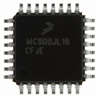
Manufacturer Part Number
MC908JL16CFJE
Description
IC MCU 16K FLASH 8MHZ 32-LQFP
Manufacturer
Freescale Semiconductor
Series
HC08r
Datasheet
1.MC908JL16CFJER.pdf
(230 pages)
Specifications of MC908JL16CFJE
Core Processor
HC08
Core Size
8-Bit
Speed
8MHz
Connectivity
I²C, SCI
Peripherals
LED, LVD, POR, PWM
Number Of I /o
26
Program Memory Size
16KB (16K x 8)
Program Memory Type
FLASH
Ram Size
512 x 8
Voltage - Supply (vcc/vdd)
2.7 V ~ 5.5 V
Data Converters
A/D 13x10b
Oscillator Type
Internal
Operating Temperature
-40°C ~ 85°C
Package / Case
32-LQFP
Processor Series
HC08JL
Core
HC08
Data Bus Width
8 bit
Data Ram Size
512 B
Interface Type
SCI
Maximum Clock Frequency
8 MHz
Number Of Programmable I/os
26
Number Of Timers
4
Operating Supply Voltage
2.7 V to 5.5 V
Maximum Operating Temperature
+ 85 C
Mounting Style
SMD/SMT
Development Tools By Supplier
FSICEBASE, DEMO908JL16E, M68CBL05CE
Minimum Operating Temperature
- 40 C
On-chip Adc
13-ch x 10-bit
Controller Family/series
HC08
No. Of I/o's
26
Ram Memory Size
512Byte
Cpu Speed
8MHz
No. Of Timers
2
Embedded Interface Type
I2C, SCI, SPI
Rohs Compliant
Yes
For Use With
DEMO908JL16E - BOARD DEMO FOR MC908JL16
Lead Free Status / RoHS Status
Lead free / RoHS Compliant
Eeprom Size
-
Lead Free Status / Rohs Status
Lead free / RoHS Compliant
Available stocks
Company
Part Number
Manufacturer
Quantity
Price
Company:

Part Number:
MC908JL16CFJE
Manufacturer:
Freescale Semiconductor
Quantity:
1 806
Company:
Part Number:
MC908JL16CFJE
Manufacturer:
Freescale Semiconductor
Quantity:
10 000
Part Number:
MC908JL16CFJE
Manufacturer:
FREESCALE
Quantity:
20 000
Company:
Part Number:
MC908JL16CFJER
Manufacturer:
Freescale Semiconductor
Quantity:
29 890
Company:
Part Number:
MC908JL16CFJER
Manufacturer:
Freescale
Quantity:
198
Company:
Part Number:
MC908JL16CFJER
Manufacturer:
Freescale Semiconductor
Quantity:
10 000


9.3.1 Clock Select and Divide Circuit
The clock select and divide circuit selects one of three clock sources and divides it by a configurable value
to generate the input clock to the converter (ADCK). The clock can be selected from one of the following
sources:
Whichever clock is selected, its frequency must fall within the acceptable frequency range for ADCK. If
the available clocks are too slow, the ADC10 will not perform according to specifications. If the available
clocks are too fast, then the clock must be divided to the appropriate frequency. This divider is specified
by the ADIV[1:0] bits and can be divide-by 1, 2, 4, or 8.
9.3.2 Input Select and Pin Control
Only one analog input may be used for conversion at any given time. The channel select bits in ADCSC
are used to select the input signal for conversion.
9.3.3 Conversion Control
Conversions can be performed in either 10-bit mode or 8-bit mode as determined by the MODE bits.
Conversions can be initiated by either a software or hardware trigger. In addition, the ADC10 module can
be configured for low power operation, long sample time, and continuous conversion.
9.3.3.1 Initiating Conversions
A conversion is initiated:
If continuous conversions are enabled a new conversion is automatically initiated after the completion of
the current conversion. In software triggered operation, continuous conversions begin after ADCSC is
written and continue until aborted. In hardware triggered operation, continuous conversions begin after a
hardware trigger event and continue until aborted.
9.3.3.2 Completing Conversions
A conversion is completed when the result of the conversion is transferred into the data result registers,
ADRH and ADRL. This is indicated by the setting of the COCO bit. An interrupt is generated if AIEN is
high at the time that COCO is set.
Freescale Semiconductor
•
•
•
•
•
•
The asynchronous clock source (ACLK) — This clock source is generated from a dedicated clock
source which is enabled when the ADC10 is converting and the clock source is selected by setting
the ACLKEN bit. When the ADLPC bit is clear, this clock operates from 1–2 MHz; when ADLPC is
set it operates at 0.5–1 MHz. This clock is not disabled in STOP and allows conversions in stop
mode for lower noise operation.
Alternate Clock Source — This clock source is equal to the external oscillator clock or a four times
the bus clock. The alternate clock source is MCU specific, see
availability of this clock source option. This clock is selected when ADICLK and ACLKEN are both
low.
The bus clock — This clock source is equal to the bus frequency. This clock is selected when
ADICLK is high and ACLKEN is low.
Following a write to ADCSC (with ADCH bits not all 1s) if software triggered operation is selected.
Following a hardware trigger event if hardware triggered operation is selected.
Following the transfer of the result to the data registers when continuous conversion is enabled.
MC68HC908JL16 Data Sheet, Rev. 1.1
Table 9-1
to determine source and
Functional Description
125
Related parts for MC908JL16CFJE
Image
Part Number
Description
Manufacturer
Datasheet
Request
R

Part Number:
Description:
Manufacturer:
Freescale Semiconductor, Inc
Datasheet:
Part Number:
Description:
Manufacturer:
Freescale Semiconductor, Inc
Datasheet:
Part Number:
Description:
Manufacturer:
Freescale Semiconductor, Inc
Datasheet:
Part Number:
Description:
Manufacturer:
Freescale Semiconductor, Inc
Datasheet:
Part Number:
Description:
Manufacturer:
Freescale Semiconductor, Inc
Datasheet:
Part Number:
Description:
Manufacturer:
Freescale Semiconductor, Inc
Datasheet:
Part Number:
Description:
Manufacturer:
Freescale Semiconductor, Inc
Datasheet:
Part Number:
Description:
Manufacturer:
Freescale Semiconductor, Inc
Datasheet:
Part Number:
Description:
Manufacturer:
Freescale Semiconductor, Inc
Datasheet:
Part Number:
Description:
Manufacturer:
Freescale Semiconductor, Inc
Datasheet:
Part Number:
Description:
Manufacturer:
Freescale Semiconductor, Inc
Datasheet:
Part Number:
Description:
Manufacturer:
Freescale Semiconductor, Inc
Datasheet:
Part Number:
Description:
Manufacturer:
Freescale Semiconductor, Inc
Datasheet:
Part Number:
Description:
Manufacturer:
Freescale Semiconductor, Inc
Datasheet:
Part Number:
Description:
Manufacturer:
Freescale Semiconductor, Inc
Datasheet: