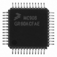
MC908GR60ACFAE Freescale Semiconductor, MC908GR60ACFAE Datasheet - Page 153

MC908GR60ACFAE
Manufacturer Part Number
MC908GR60ACFAE
Description
IC MCU 60K FLASH 8MHZ 48-LQFP
Manufacturer
Freescale Semiconductor
Series
HC08r
Datasheet
1.MC908GR32ACFJE.pdf
(314 pages)
Specifications of MC908GR60ACFAE
Core Processor
HC08
Core Size
8-Bit
Speed
8MHz
Connectivity
SCI, SPI
Peripherals
LVD, POR, PWM
Number Of I /o
37
Program Memory Size
60KB (60K x 8)
Program Memory Type
FLASH
Ram Size
2K x 8
Voltage - Supply (vcc/vdd)
3 V ~ 5.5 V
Data Converters
A/D 24x10b
Oscillator Type
Internal
Operating Temperature
-40°C ~ 85°C
Package / Case
48-LQFP
Controller Family/series
HC08
No. Of I/o's
37
Ram Memory Size
2KB
Cpu Speed
8MHz
No. Of Timers
2
Embedded Interface Type
SCI, SPI
Rohs Compliant
Yes
Processor Series
HC08GR
Core
HC08
Data Bus Width
8 bit
Data Ram Size
2 KB
Interface Type
ESCI, SPI
Maximum Clock Frequency
8 MHz
Number Of Programmable I/os
53
Number Of Timers
8
Maximum Operating Temperature
+ 85 C
Mounting Style
SMD/SMT
Development Tools By Supplier
FSICEBASE, DEMO908GZ60E, M68CBL05CE, M68EML08GPGTE
Minimum Operating Temperature
- 40 C
On-chip Adc
10 bit, 24 Channel
Lead Free Status / RoHS Status
Lead free / RoHS Compliant
Eeprom Size
-
Lead Free Status / Rohs Status
Details
Available stocks
Company
Part Number
Manufacturer
Quantity
Price
Company:
Part Number:
MC908GR60ACFAE
Manufacturer:
Freescale Semiconductor
Quantity:
10 000
Part Number:
MC908GR60ACFAE
Manufacturer:
FREESCALE
Quantity:
20 000
- Current page: 153 of 314
- Download datasheet (5Mb)
13.3 Pin Name Conventions
The generic names of the ESCI input/output (I/O) pins are:
ESCI I/O lines are implemented by sharing parallel I/O port pins. The full name of an ESCI input or output
reflects the name of the shared port pin.
ESCI I/O pins. The generic pin names appear in the text of this section.
13.4 Functional Description
Figure 13-3
serial communication between the MCU and remote devices, including other MCUs. The transmitter and
receiver of the ESCI operate independently, although they use the same baud rate generator. During
normal operation, the CPU monitors the status of the ESCI, writes the data to be transmitted, and
processes received data.
The baud rate clock source for the ESCI can be selected via the configuration bit, SCIBDSRC, of the
CONFIG2 register ($001E)
For reference, a summary of the ESCI module input/output registers is provided in
13.4.1 Data Format
The SCI uses the standard non-return-to-zero mark/space data format illustrated in
Freescale Semiconductor
•
•
RxD (receive data)
TxD (transmit data)
shows the structure of the ESCI module. The ESCI allows full-duplex, asynchronous, NRZ
START
START
MC68HC908GR60A • MC68HC908GR48A • MC68HC908GR32A Data Sheet, Rev. 5
BIT
BIT
Generic Pin Names
BIT 0
BIT 0
Full Pin Names
BIT 1
BIT 1
Table 13-1. Pin Name Conventions
BIT 2
BIT 2
Figure 13-2. SCI Data Formats
BIT 3
BIT 3
Table 13-1
(BIT M IN SCC1 CLEAR)
9-BIT DATA FORMAT
(BIT M IN SCC1 SET)
8-BIT DATA FORMAT
BIT 4
BIT 4
PTE1/RxD
RxD
BIT 5
BIT 5
shows the full names and the generic names of the
BIT 6
BIT 6
OR DATA
PARITY
BIT 7
BIT 7
BIT
OR DATA
PARITY
PTE0/TxD
STOP
BIT 8
BIT
BIT
TxD
START
NEXT
STOP
BIT
BIT
START
NEXT
BIT
Figure
Pin Name Conventions
Figure
13-4.
13-2.
153
Related parts for MC908GR60ACFAE
Image
Part Number
Description
Manufacturer
Datasheet
Request
R
Part Number:
Description:
Manufacturer:
Freescale Semiconductor, Inc
Datasheet:
Part Number:
Description:
Manufacturer:
Freescale Semiconductor, Inc
Datasheet:
Part Number:
Description:
Manufacturer:
Freescale Semiconductor, Inc
Datasheet:
Part Number:
Description:
Manufacturer:
Freescale Semiconductor, Inc
Datasheet:
Part Number:
Description:
Manufacturer:
Freescale Semiconductor, Inc
Datasheet:
Part Number:
Description:
Manufacturer:
Freescale Semiconductor, Inc
Datasheet:
Part Number:
Description:
Manufacturer:
Freescale Semiconductor, Inc
Datasheet:
Part Number:
Description:
Manufacturer:
Freescale Semiconductor, Inc
Datasheet:
Part Number:
Description:
Manufacturer:
Freescale Semiconductor, Inc
Datasheet:
Part Number:
Description:
Manufacturer:
Freescale Semiconductor, Inc
Datasheet:
Part Number:
Description:
Manufacturer:
Freescale Semiconductor, Inc
Datasheet:
Part Number:
Description:
Manufacturer:
Freescale Semiconductor, Inc
Datasheet:
Part Number:
Description:
Manufacturer:
Freescale Semiconductor, Inc
Datasheet:
Part Number:
Description:
Manufacturer:
Freescale Semiconductor, Inc
Datasheet:
Part Number:
Description:
Manufacturer:
Freescale Semiconductor, Inc
Datasheet:


