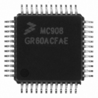
MC908GR60ACFAE Freescale Semiconductor, MC908GR60ACFAE Datasheet - Page 69

MC908GR60ACFAE
Manufacturer Part Number
MC908GR60ACFAE
Description
IC MCU 60K FLASH 8MHZ 48-LQFP
Manufacturer
Freescale Semiconductor
Series
HC08r
Datasheet
1.MC908GR32ACFJE.pdf
(314 pages)
Specifications of MC908GR60ACFAE
Core Processor
HC08
Core Size
8-Bit
Speed
8MHz
Connectivity
SCI, SPI
Peripherals
LVD, POR, PWM
Number Of I /o
37
Program Memory Size
60KB (60K x 8)
Program Memory Type
FLASH
Ram Size
2K x 8
Voltage - Supply (vcc/vdd)
3 V ~ 5.5 V
Data Converters
A/D 24x10b
Oscillator Type
Internal
Operating Temperature
-40°C ~ 85°C
Package / Case
48-LQFP
Controller Family/series
HC08
No. Of I/o's
37
Ram Memory Size
2KB
Cpu Speed
8MHz
No. Of Timers
2
Embedded Interface Type
SCI, SPI
Rohs Compliant
Yes
Processor Series
HC08GR
Core
HC08
Data Bus Width
8 bit
Data Ram Size
2 KB
Interface Type
ESCI, SPI
Maximum Clock Frequency
8 MHz
Number Of Programmable I/os
53
Number Of Timers
8
Maximum Operating Temperature
+ 85 C
Mounting Style
SMD/SMT
Development Tools By Supplier
FSICEBASE, DEMO908GZ60E, M68CBL05CE, M68EML08GPGTE
Minimum Operating Temperature
- 40 C
On-chip Adc
10 bit, 24 Channel
Lead Free Status / RoHS Status
Lead free / RoHS Compliant
Eeprom Size
-
Lead Free Status / Rohs Status
Details
Available stocks
Company
Part Number
Manufacturer
Quantity
Price
Company:
Part Number:
MC908GR60ACFAE
Manufacturer:
Freescale Semiconductor
Quantity:
10 000
Part Number:
MC908GR60ACFAE
Manufacturer:
FREESCALE
Quantity:
20 000
- Current page: 69 of 314
- Download datasheet (5Mb)
3.8.2.4 Eight Bit Truncation Mode
In 8-bit truncation mode, the ADRL register holds the eight MSBs of the 10-bit result. The ADRH register
is unused and reads as 0. The ADRL register is updated each time an ADC single channel conversion
completes. In 8-bit mode, the ADRL register contains no interlocking with ADRH.
3.8.3 ADC Clock Register
The ADC clock register (ADCLK) selects the clock frequency for the ADC.
ADIV2–ADIV0 — ADC Clock Prescaler Bits
Freescale Semiconductor
ADIV2–ADIV0 form a 3-bit field which selects the divide ratio used by the ADC to generate the internal
ADC clock.
approximately 1 MHz.
Address:
Address:
Address:
Table 3-2
Reset:
Reset:
Reset:
Read:
Read:
Read:
Write:
Write:
Write:
MC68HC908GR60A • MC68HC908GR48A • MC68HC908GR32A Data Sheet, Rev. 5
Figure 3-8. ADC Data Register High (ADRH) and Low (ADRL)
$003D
$003E
ADIV2
$003F
Bit 7
AD9
Bit 7
1. X = Don’t care
0
0
shows the available clock configurations. The ADC clock should be set to
ADIV2
0
0
0
0
1
Figure 3-9. ADC Clock Register (ADCLK)
= Unimplemented
= Unimplemented
ADIV1
AD8
6
0
6
0
Table 3-2. ADC Clock Divide Ratio
ADIV1
X
0
0
1
1
(1)
ADIV0
AD7
5
0
5
0
ADIV0
X
0
1
0
1
(1)
ADICLK
Unaffected by reset
Unaffected by reset
AD6
R
4
0
4
0
ADC input clock ÷ 1
ADC input clock ÷ 2
ADC input clock ÷ 4
ADC input clock ÷ 8
ADC input clock ÷ 16
= Reserved
MODE1
AD5
3
0
3
0
ADC Clock Rate
MODE0
AD4
2
0
2
1
AD3
R
1
0
1
0
ADRH
ADRL
Bit 0
AD2
Bit 0
0
0
0
I/O Registers
69
Related parts for MC908GR60ACFAE
Image
Part Number
Description
Manufacturer
Datasheet
Request
R
Part Number:
Description:
Manufacturer:
Freescale Semiconductor, Inc
Datasheet:
Part Number:
Description:
Manufacturer:
Freescale Semiconductor, Inc
Datasheet:
Part Number:
Description:
Manufacturer:
Freescale Semiconductor, Inc
Datasheet:
Part Number:
Description:
Manufacturer:
Freescale Semiconductor, Inc
Datasheet:
Part Number:
Description:
Manufacturer:
Freescale Semiconductor, Inc
Datasheet:
Part Number:
Description:
Manufacturer:
Freescale Semiconductor, Inc
Datasheet:
Part Number:
Description:
Manufacturer:
Freescale Semiconductor, Inc
Datasheet:
Part Number:
Description:
Manufacturer:
Freescale Semiconductor, Inc
Datasheet:
Part Number:
Description:
Manufacturer:
Freescale Semiconductor, Inc
Datasheet:
Part Number:
Description:
Manufacturer:
Freescale Semiconductor, Inc
Datasheet:
Part Number:
Description:
Manufacturer:
Freescale Semiconductor, Inc
Datasheet:
Part Number:
Description:
Manufacturer:
Freescale Semiconductor, Inc
Datasheet:
Part Number:
Description:
Manufacturer:
Freescale Semiconductor, Inc
Datasheet:
Part Number:
Description:
Manufacturer:
Freescale Semiconductor, Inc
Datasheet:
Part Number:
Description:
Manufacturer:
Freescale Semiconductor, Inc
Datasheet:


