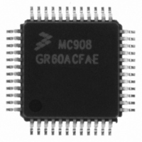
MC908GR60ACFAE Freescale Semiconductor, MC908GR60ACFAE Datasheet - Page 209

MC908GR60ACFAE
Manufacturer Part Number
MC908GR60ACFAE
Description
IC MCU 60K FLASH 8MHZ 48-LQFP
Manufacturer
Freescale Semiconductor
Series
HC08r
Datasheet
1.MC908GR32ACFJE.pdf
(314 pages)
Specifications of MC908GR60ACFAE
Core Processor
HC08
Core Size
8-Bit
Speed
8MHz
Connectivity
SCI, SPI
Peripherals
LVD, POR, PWM
Number Of I /o
37
Program Memory Size
60KB (60K x 8)
Program Memory Type
FLASH
Ram Size
2K x 8
Voltage - Supply (vcc/vdd)
3 V ~ 5.5 V
Data Converters
A/D 24x10b
Oscillator Type
Internal
Operating Temperature
-40°C ~ 85°C
Package / Case
48-LQFP
Controller Family/series
HC08
No. Of I/o's
37
Ram Memory Size
2KB
Cpu Speed
8MHz
No. Of Timers
2
Embedded Interface Type
SCI, SPI
Rohs Compliant
Yes
Processor Series
HC08GR
Core
HC08
Data Bus Width
8 bit
Data Ram Size
2 KB
Interface Type
ESCI, SPI
Maximum Clock Frequency
8 MHz
Number Of Programmable I/os
53
Number Of Timers
8
Maximum Operating Temperature
+ 85 C
Mounting Style
SMD/SMT
Development Tools By Supplier
FSICEBASE, DEMO908GZ60E, M68CBL05CE, M68EML08GPGTE
Minimum Operating Temperature
- 40 C
On-chip Adc
10 bit, 24 Channel
Lead Free Status / RoHS Status
Lead free / RoHS Compliant
Eeprom Size
-
Lead Free Status / Rohs Status
Details
Available stocks
Company
Part Number
Manufacturer
Quantity
Price
Company:
Part Number:
MC908GR60ACFAE
Manufacturer:
Freescale Semiconductor
Quantity:
10 000
Part Number:
MC908GR60ACFAE
Manufacturer:
FREESCALE
Quantity:
20 000
- Current page: 209 of 314
- Download datasheet (5Mb)
15.5 Queuing Transmission Data
The double-buffered transmit data register allows a data byte to be queued and transmitted. For an SPI
configured as a master, a queued data byte is transmitted immediately after the previous transmission
has completed. The SPI transmitter empty flag (SPTE) indicates when the transmit data buffer is ready
to accept new data. Write to the transmit data register only when SPTE is high.
timing associated with doing back-to-back transmissions with the SPI (SPSCK has CPHA: CPOL = 1:0).
The transmit data buffer allows back-to-back transmissions without the slave precisely timing its writes
between transmissions as in a system with a single data buffer. Also, if no new data is written to the data
buffer, the last value contained in the shift register is the next data word to be transmitted.
For an idle master or idle slave that has no data loaded into its transmit buffer, the SPTE is set again no
more than two bus cycles after the transmit buffer empties into the shift register. This allows the user to
queue up a 16-bit value to send. For an already active slave, the load of the shift register cannot occur
until the transmission is completed. This implies that a back-to-back write to the transmit data register is
not possible. SPTE indicates when the next write can occur.
Freescale Semiconductor
CPHA:CPOL = 1:0
WRITE TO SPDR
4 FIRST INCOMING BYTE TRANSFERS FROM SHIFT
5
1
2
3
6 CPU READS SPSCR WITH SPRF BIT SET.
READ SPSCR
CPU WRITES BYTE 1 TO SPDR, CLEARING SPTE BIT.
BYTE 1 TRANSFERS FROM TRANSMIT DATA
REGISTER TO SHIFT REGISTER, SETTING SPTE BIT.
CPU WRITES BYTE 2 TO SPDR, QUEUEING BYTE 2
AND CLEARING SPTE BIT.
REGISTER TO RECEIVE DATA REGISTER, SETTING
SPRF BIT.
BYTE 2 TRANSFERS FROM TRANSMIT DATA
REGISTER TO SHIFT REGISTER, SETTING SPTE BIT.
READ SPDR
MC68HC908GR60A • MC68HC908GR48A • MC68HC908GR32A Data Sheet, Rev. 5
SPSCK
SPRF
SPTE
MOSI
1
Figure 15-9. SPRF/SPTE CPU Interrupt Timing
MSB BIT
BYTE 1
2
6
BIT
5
3
BIT
4
BIT
3
BIT
2
BIT
1
10
11 CPU READS SPSCR WITH SPRF BIT SET.
12 CPU READS SPDR, CLEARING SPRF BIT.
7 CPU READS SPDR, CLEARING SPRF BIT.
8
9
LSB MSB BIT
5
4
CPU WRITES BYTE 3 TO SPDR, QUEUEING BYTE
3 AND CLEARING SPTE BIT.
SECOND INCOMING BYTE TRANSFERS FROM SHIFT
REGISTER TO RECEIVE DATA REGISTER, SETTING
SPRF BIT.
BYTE 3 TRANSFERS FROM TRANSMIT DATA
REGISTER TO SHIFT REGISTER, SETTING SPTE BIT.
BYTE 2
6
6
7
BIT
5
8
BIT
4
BIT
3
BIT
2
BIT
1
LSB MSB BIT
10
9
Queuing Transmission Data
BYTE 3
Figure 15-9
11
6
12
BIT
5
BIT
4
shows the
209
Related parts for MC908GR60ACFAE
Image
Part Number
Description
Manufacturer
Datasheet
Request
R
Part Number:
Description:
Manufacturer:
Freescale Semiconductor, Inc
Datasheet:
Part Number:
Description:
Manufacturer:
Freescale Semiconductor, Inc
Datasheet:
Part Number:
Description:
Manufacturer:
Freescale Semiconductor, Inc
Datasheet:
Part Number:
Description:
Manufacturer:
Freescale Semiconductor, Inc
Datasheet:
Part Number:
Description:
Manufacturer:
Freescale Semiconductor, Inc
Datasheet:
Part Number:
Description:
Manufacturer:
Freescale Semiconductor, Inc
Datasheet:
Part Number:
Description:
Manufacturer:
Freescale Semiconductor, Inc
Datasheet:
Part Number:
Description:
Manufacturer:
Freescale Semiconductor, Inc
Datasheet:
Part Number:
Description:
Manufacturer:
Freescale Semiconductor, Inc
Datasheet:
Part Number:
Description:
Manufacturer:
Freescale Semiconductor, Inc
Datasheet:
Part Number:
Description:
Manufacturer:
Freescale Semiconductor, Inc
Datasheet:
Part Number:
Description:
Manufacturer:
Freescale Semiconductor, Inc
Datasheet:
Part Number:
Description:
Manufacturer:
Freescale Semiconductor, Inc
Datasheet:
Part Number:
Description:
Manufacturer:
Freescale Semiconductor, Inc
Datasheet:
Part Number:
Description:
Manufacturer:
Freescale Semiconductor, Inc
Datasheet:


