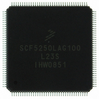
SCF5250LAG100 Freescale Semiconductor, SCF5250LAG100 Datasheet - Page 13

SCF5250LAG100
Manufacturer Part Number
SCF5250LAG100
Description
IC MPU COLDFIRE 100MHZ 144-LQFP
Manufacturer
Freescale Semiconductor
Series
SCF52xxr
Datasheet
1.SCFLXRAYADPTS12.pdf
(56 pages)
Specifications of SCF5250LAG100
Core Processor
Coldfire V2
Core Size
32-Bit
Speed
100MHz
Connectivity
EBI/EMI, I²C, IDE, MMC, SPI, UART/USART
Peripherals
DMA, I²S, POR, Serial Audio, WDT
Number Of I /o
57
Program Memory Type
ROMless
Ram Size
128K x 8
Voltage - Supply (vcc/vdd)
1.08 V ~ 1.32 V
Data Converters
A/D 6x12b
Oscillator Type
Internal
Operating Temperature
-20°C ~ 70°C
Package / Case
144-LQFP
Eeprom Size
-
Program Memory Size
-
Available stocks
Company
Part Number
Manufacturer
Quantity
Price
Company:
Part Number:
SCF5250LAG100
Manufacturer:
Intersil
Quantity:
90
Company:
Part Number:
SCF5250LAG100
Manufacturer:
Freescale Semiconductor
Quantity:
10 000
Part Number:
SCF5250LAG100
Manufacturer:
FREESCALE
Quantity:
20 000
3.2.2
This signal indicates during any bus cycle whether a read or write is in progress. A low is write cycle and
a high is a read cycle.
3.2.3
The OE signal is intended to be connected to the output enable of asynchronous memories connected to
chip selects. During bus read cycles, the ColdFire processor will drive OE low.
3.2.4
The data bus (D[31:16]) is bi-directional and non-multiplexed. Data is registered by the SCF5250 on the
rising clock edge. The data bus uses a default configuration if none of the chip-selects or DRAM bank
match the address decode. All 16 bits of the data bus are driven during writes, regardless of port width or
operand size.
3.2.5
The TA/GPIO12 pin is the transfer acknowledge signal.
3.3
The following SDRAM signals provide a glueless interface to external SDRAM. An SDRAM width of 16
bits is supported and can access as much as 32MB of memory. ADRAMs are not supported.
Freescale Semiconductor
Synchronous DRAM row address strobe
Synchronous DRAM UDQM and LQDM
Synchronous DRAM Column Address
Synchronous DRAM Clock Enable
Synchronous DRAM Chip Enable
Synchronous DRAM clock
Synchronous DRAM Write
SDRAM Controller Signals
SDRAM Signal
Read-Write Control
Output Enable
Data Bus
Transfer Acknowledge
signals
Strobe
SCF5250 Data Sheet:
Table 3. SDRAM Controller Signals
The BCLKE active high output signal is used during synchronous mode to route
The SDRAS/GPIO59 active low pin provides a seamless interface to the RAS input
on synchronous DRAM
The SDCAS/GPIO39 active low pin provides a seamless interface to CAS input on
synchronous DRAM.
The SDWE/GPIO38 active-low pin is asserted to signify that a SDRAM write cycle
is underway. This pin outputs logic ‘1’ during read bus cycles.
The SD_CS0/GPIO60 active-low output signal is used during synchronous mode
to route directly to the chip select of a SDRAM device.
The DRAM byte enables UDMQ and LDQM are driven by the SDUDQM/GPO53
and SDLDQM/GPO52 byte enable outputs.
The DRAM clock is driven by the BCLK/GPIO40 signal
directly to the SCKE signal of external SDRAMs. This signal provides the clock
enable to the SDRAM.
Technical
Data,
Rev. 1.3
Description
13


