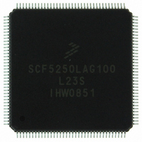
SCF5250LAG100 Freescale Semiconductor, SCF5250LAG100 Datasheet - Page 17

SCF5250LAG100
Manufacturer Part Number
SCF5250LAG100
Description
IC MPU COLDFIRE 100MHZ 144-LQFP
Manufacturer
Freescale Semiconductor
Series
SCF52xxr
Datasheet
1.SCFLXRAYADPTS12.pdf
(56 pages)
Specifications of SCF5250LAG100
Core Processor
Coldfire V2
Core Size
32-Bit
Speed
100MHz
Connectivity
EBI/EMI, I²C, IDE, MMC, SPI, UART/USART
Peripherals
DMA, I²S, POR, Serial Audio, WDT
Number Of I /o
57
Program Memory Type
ROMless
Ram Size
128K x 8
Voltage - Supply (vcc/vdd)
1.08 V ~ 1.32 V
Data Converters
A/D 6x12b
Oscillator Type
Internal
Operating Temperature
-20°C ~ 70°C
Package / Case
144-LQFP
Eeprom Size
-
Program Memory Size
-
Available stocks
Company
Part Number
Manufacturer
Quantity
Price
Company:
Part Number:
SCF5250LAG100
Manufacturer:
Intersil
Quantity:
90
Company:
Part Number:
SCF5250LAG100
Manufacturer:
Freescale Semiconductor
Quantity:
10 000
Part Number:
SCF5250LAG100
Manufacturer:
FREESCALE
Quantity:
20 000
3.12
There is a 3-line subcode interface on the SCF5250 processor. This 3-line subcode interface allows the
device to format and transmit subcode in EIAJ format to a CD channel encoder device. The three signals
are described in
3.13
The ADOUT signal on the ADOUT/SCLK4/GPIO58 pin provides the reference voltage in PWM format.
This output requires an external integrator circuit (resistor/capacitor) to convert it to a DC level to be input
to the ADREF pin.
The six AD inputs are each fed to their own comparator. The reference input to each (ADREF) is then
multiplexed as only one AD comparison can be made at any one time.
3.14
The device has a versatile flash card interface that supports both Secure Digital and Memory Stick cards.
The interface can either support one Secure Digital or two Memory Stick cards. No mixing of card types
is possible.
Freescale Semiconductor
RCK/QSPI_DIN/QSPI_DOUT/GPIO26 Subcode clock input. When pin is used as subcode clock, this pin is driven by the CD
EBUIN3/CMD_SDIO2/GPIO14
QSPI_DOUT/SFSY/GPIO27
QSPI_CLK/SUBR/GPIO25
EBUIN2/SCLKOUT/GPIO13
Flash Memory Signal
Subcode Interface
Analog to Digital Converter (ADC)
Secure Digital/Memory Stick Card Interface
Signal name
To use the ADINx as General Purpose inputs (rather than there analogue function) it is
necessary to generate a fixed comparator voltage level of VDD/2. This can be
accomplished by a potential divider network connected to the ADREF pin. However in
portable applications where stand-by power consumption is important the current taken
by the divider network (in stand-by mode) could be excessive. Therefore it is possible to
generate a VDD/2 voltage by selecting SCLK4 output mode and feeding this clock signal
(which is 50% duty cycle) through an external integration circuit. This would generate a
voltage level equal to VDD/2 but would be disabled when stand-by mode was selected.
Table 10
Table
gives the pin descriptions.
9.
SCF5250 Data Sheet:
channel encoder.
Subcode sync output
This signal is driven high if a subcode sync needs to be inserted in the EFM stream.
Subcode data output
This signal is a subcode data out pin.
Table 10. Flash Memory Card Signals
Clock out for both Memory Stick interfaces and for Secure Digital
Secure Digital command line
Memory Stick interface 2 data I/O
Table 9. Subcode Interface Signal
NOTE
Technical
Data,
Description
Description
Rev. 1.3
17


